
Download this article in .PDF format
This file type includes high resolution graphics and schematics.
Delta-sigma analog-to-digital converters (ADCs) are fascinating—almost mythical in their ability to support low- to medium-speed and high-resolution applications. They take advantage of the speed of analog circuits, along with the robustness of digital circuits. They also reduce the amount of analog circuitry used in the converter. More importantly, the analog parts of the circuit don’t need to be very accurate. Of course, the digital blocks then must work at higher sampling clocks and, thus, consume more power.
Table Of Contents
- Delta-Sigma Modulators
- Quantization Noise
- Oversampling
- Oversampling’s Effect On Noise
- Noise Shaping
- How The Modulator Works
- Oversampling’s Effect On SNR
- Effect Of Higher-Order Modulators On SNR
- Higher-Order Modulators
- References
Delta-Sigma Modulators
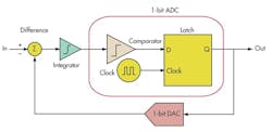
A delta-sigma ADC generally comprises a delta-sigma modulator, followed by a decimation filter. Delta-sigma modulation is one of the most effective forms of conversion in the data converter world. Its applications include communication systems, professional audio, and precision measurements.
The goal of delta-sigma modulation is to achieve higher transmission efficiency by transmitting only the changes (delta) in value between consecutive samples, rather than the actual samples themselves. ADCs and digital-to-analog converters (DACs) both can use delta-sigma modulation.
Oversampling reduces the effect of noise within the signal bandwidth of interest, benefitting the delta-sigma ADC’s analog operation. Next, noise shaping pushes the noise out of signal bandwidth. Digital operation then filters out the noise that’s out of the band of interest. Finally, this digital filter decimates or down-samples the data. Before considering the modulator itself, though, it’s necessary to become familiar with a few concepts that play a significant role in converters: quantization noise, oversampling, and noise shaping.
Quantization Noise
In an ADC, the quantized signal can be described as the input signal plus quantization noise:
VQuantized = VIn + ε
(1)
VQuantized and VIn are, respectively, the quantized signal and the input signal; εis the error associated with this process, or the difference between the input and output of the quantizer.
The converter’s full range divided by the number of its quantization levels defines its least significant bit (LSB). An N-bit converter has 2N levels of quantization. Therefore, the width of any of these quantization levels is FS/(2N – 1). For an ADC with a quantization width of ∆, the quantization noise has equal probability of falling anywhere between –∆/2 and +∆/2 and a probability density function that is uniform over the range of quantization error. The quantization noise power can be calculated by integrating the error over this range as in:

(2)
which describes the noise power in terms of LSB width. However, it can be rewritten to express it in terms of number of bits and full scale:


(4)
Under oversampled conditions, the noise power that falls within the signal bandwidth (0 to fO) is given by:

(5)
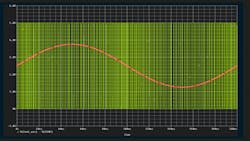
As the equation illustrates, oversampling reduces the in-band rms noise by the square root of the oversampling ratio (Fig. 1).
The reduction is quantified in:

While oversampling the input to the converter reduces noise, this reduction is even greater for delta-sigma modulators. In fact, higher-order modulators can further decrease noise.1 The general formula for calculating the noise of a modulator with an order of L and OSR of M is given by:

(7)
Note that Equation 6 could be obtained from Equation 7 for the case in which no delta-sigma modulation is used. In that case, the order of modulation would be considered zero.
Noise Shaping
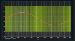
By oversampling, the noise spectrum is distributed over a wider frequency range. The next step in a sigma-delta is shaping the noise and pushing most of the noise spectrum to higher frequencies so the in-band noise is reduced significantly. This concept is called noise shaping (Fig. 2).
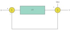
This simple feedback system can be represented by:

(8)

(9)
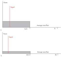
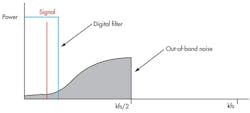
Note that in Equation 9, as frequency approaches zero, Y approaches input component X. As the frequency increases, the first term (with the input signal component) approaches zero, and the output approaches Q(n). In other words, at high frequencies, the output consists mostly of quantization noise. Overall, it seems as if a low-pass filter is acting on the signal in the forward path and a high-pass filter is acting on noise in the feedback path. Noise shaping has been achieved! After that, all that needs to be done is to filter out the noise at high frequencies (Fig. 3).
Oversampling’s Effect On SNR
Oversampling improves signal-to-noise ratio (SNR). When noise power is reduced, an increase in SNR is expected. From a quantitative point of view, starting with the quantization noise for non-oversampled converters obtained by Equation 2, the theoretical SNR value for quantized noise is expressed by the ratio of input signal to noise signal:

(10)

(11)
where N is the number of bits in the converter. Equation 6 expresses the noise power for an oversampled converter. Using Equations 6 and 10, the SNR for a converter with an over-sampling ratio of OSR could be calculated as:
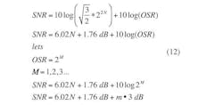
(12)
SNR improves by 3 dB, or 0.5 bit, each time the sampling frequency is doubled. For example, a 16-bit converter has a theoretical value for SNR of about 98 dB. But with an oversampling ratio of 8, the SNR is increased to 107 dB for an increase of 3 dB/octave, or 9 dB in total.
Effect Of Higher-Order Modulators On SNR
Using higher-order modules, delta-sigma will further improve SNR. A second-order modulator improves SNR by 15 dB for each doubling of oversampling ratio. The improvement that is achieved for each doubling of oversampling ratio generally can be calculated from:
3(2L + 1)dB
(13)
for each doubling of OSR. Equation 13 also shows that for a first-order modulator (where L = 1), there is a 9-dB improvement for every oversampling ratio of two. For a second-order modulator (L = 2) with the same OSR, this improvement increases to 15 dB—that is, there is a 6-dB improvement for each additional order of modulator.
Higher-Order Modulators
Since the modulator’s output is a digital bit stream, it is hard to visualize and check the correctness of the digitized input signal at its output (Fig. 5 and table).
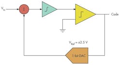
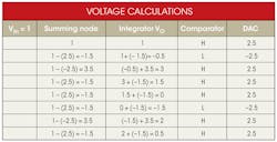
For example, code 10111011 is obtained by reading the comparator’s output for each comparison. The full scale in this example is (2.5 – (–2 .5)) = 5 V.
On a 5-V scale, because the lower reference is sitting at –2.5 V, a 1-V signal will be 3.5 V above the lower reference. This is 0.7 of the full scale (3.5/5 = 0.7). The resulting code (HLHHHLHH or 10111011) has six highs and two lows, so six out of eight of the bit-stream codes are high. Thus, the average value is 6/8 = 0.75. This average value is close to the actual value of the input (0.7).
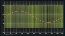
If one continues the operation and obtains more bits for the table, the average value gets closer and closer to 0.7. For this type of modulator, it is understood that for values that are closer to +VRef, the modulator generates more highs. For input values that are closer to –VRef, the modulator generates more lows. A typical sine-wave input generates a code that has more highs or lows at its two peaks. As the input gets closer to the mid-range, on average, the resulting number of ones and zeros becomes comparable (Fig. 6).
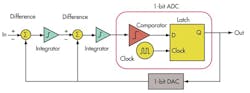
Typically, the modulator takes an order that is greater than one (Fig. 7).
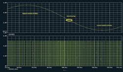
The bit stream output by the model of a sixth-order modulator is followed by a decimation filter to form a 24-bit delta-sigma ADC, resulting in this output. Again, as the input amplitude is increased, the modulator generates more ones and, moving toward the lowest voltage of the input, more zeros (Fig. 8).
References
1. Delta-Sigma Data Converters; Theroy, Design, and Simulation, S.R. Norseworthy, R. Schreier, G.C. Temes, Wiley Interscience, 1997.
2. “A Sigma-Delta Modulator as an A/D Converter,” R.J. Van de Plassche, IEEE Transactions on Circuits and Systems, Vol. CAS-25, July 1978, pp. 510-514.
3. “Principles of Oversampling A/D Conversion,” Max W. Hauser, Journal Audio Engineering Society, Vol. 39, No. 1/2, January/February 1991, pp. 3-26.
4. “On Design & Implementation of a Decimation Filter for Multi-standard Wireless Transceivers,” A. Ghaze & et al., IEEE Transactions of Wireless Communications, Vol. 1, No. 4, Oct. 02.
5. “Understanding Cascaded Integrator Comb Filters,”Richard Lyons, Embedded Systems Programming, March 2005, www.design-reuse.com/articles/10028/understanding-cascaded-integrator-comb-filters.html
6. “An Economical Class of Digital Filters for Decimation and Interpolation,” E.B. Hogenauer, IEEE Transactions on Acoustics, Speech, and Signal Processing, Vol. 29, No. 2, April 1981, pp 155-162
7. “Design Tradeoffs for Linear Phase FIR Decimation Filters and ∑-∂ Modulators,” A. Blad, P. Lowenborg, H. Johansson, 14th European Signal Processing Conference, 2006
8. “Low power Decimation Filter Architectures for ∑-∂ ADCs,” Özge Gürsoy, Orkun Sağlamdemir, Mustafa Aktan, Selçuk Talay, Günhan Dündar
9. For more information on data converters, visit www.ti.com/dataconverters-ca.
Download this article in .PDF format
This file type includes high resolution graphics and schematics.
About the Author
Arash Loloee
Member, Group Technical Staff
Arash Loloee is a member of TI’s Group Technical Staff. As Senior IC Design Engineer, he is responsible for designing transistor- to system-level projects. He received his PhD in EE and MSEE from Southern Methodist University and his BS in physics from the University of North Texas. He also was a lecturer at the University of Texas at Dallas from 2005 to 2011, where he taught various analog-related topics. He has three patents, with one pending. He can be reached at [email protected].
Comment About the Article
To join the conversation, and become an exclusive member of Electronic Design, create an account today!

Leaders relevant to this article: