Understanding Spurious-Free Dynamic Range In Wideband GSPS ADCs

Many analog input specifications should be considered in selecting a wideband analog-to-digital converter (ADC) for a high-performance system, such as ADC resolution, sample rate, signal-to-noise ratio (SNR), effective number of bits (ENOB), input bandwidth, spurious free dynamic range (SFDR), and differential or integral non-linearity.
This file type includes high resolution graphics and schematics when applicable.
For gigasample-per-second (GSPS) ADCs, perhaps one of the most important ac performance specifications is SFDR. It simply defines the capability of the ADC, and the system, to decipher a carrier signal from other noise or any other spurious frequency.
To achieve the conversion speed used in GSPS ADCs, several architectures that capture signals at a high sample rate of interest can be employed. However, some of these architectures are used at the expense of full-bandwidth SFDR performance.
To understand the impact of the converter SFDR on the system, we answered some common questions from design engineers about the details of the SFDR specification, how it is described in converter datasheets, the architectures that limit or maximize the ADC performance, and system design aspects that limit SFDR performance.
I have seen SFDR stated in datasheets with and without caveats. What exactly is SFDR?
Being able to discern a signal from the noise is a key aspect of many signal acquisition systems. Whether it is a defined telecommunications protocol, a radar sweep, or measurement instrumentation, acquiring and deciphering weak signals is at the heart of any differentiating system performance.
SFDR represents the smallest power signal that can be distinguished from a large interfering signal. It defines the dynamic ratio between the root mean square (rms) value of the power of a carrier and the rms value of the next most significant spurious signal seen in the frequency domain, such as in a fast Fourier transform (FFT). Hence, by definition, this dynamic range must be free of other spurious frequencies, or spurs.
SFDR is often quantified as the range, in units of power (dBc), relative from the carrier of interest to the power of the next most significant frequency. However, it also could be referenced to a full-scale signal in units of power (dBFS). This is an important distinction since the carrier of interest may be a relatively lower-power signal that is well below the full-scale input to the ADC. When this is the case, the SFDR becomes paramount in distinguishing the signal from other noise and spurious frequencies.
What limits the SFDR of an ADC?
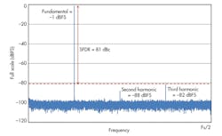
A harmonic frequency is an integer multiple of the fundamental frequency. For a well-designed monolithic ADC core, the SFDR typically will be dominated by the dynamic range between a carrier frequency and the second or third harmonic of the fundamental frequency of interest. Some narrowband ADC datasheets will define the SFDR only in the narrow band of operation, typically when the second and third harmonics fall out of band. Other datasheets may describe SFDR over a wide bandwidth with caveats as to what conditions need to exist for this performance.
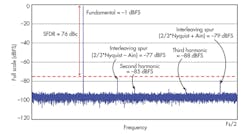
Although the second or third harmonic may typically be the dominant spurious frequency, there are spurs that could also limit the SFDR performance of a GSPS ADC due to other system reasons. For example, multiple interleaved ADC cores can create spurious frequencies by the introduction of interleaving artifacts into the frequency domain. These can have the potential to be larger in magnitude than the second or third harmonic of the fundamental frequency. Therefore, they would be the dominant limiting factor for SFDR. Although it may seem counterintuitive, SFDR could also be specified in an interleaved ADC datasheet with the admonition that interleaving spurs are excluded from the calculation (Fig. 1).
Can narrowband SFDR be extrapolated to wideband SFDR?
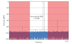
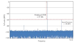
If only a narrow band of spectrum is of interest for the system, a band-pass anti-aliasing input filter can be used to suppress the harmonics or artifacts that are outside the band of interest. This may work fine for some applications, as long as the there is no need to observe signals within this filtered frequency band. But for a wideband signal acquisition system, this is not feasible. On some datasheets, an ADC’s SFDR also could be specified over a narrow slice of bandwidth that is much less than the full input bandwidth of the ADC.
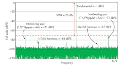
Typically, it cannot be assumed that the SFDR across a narrow frequency band can be extrapolated to get the same performance across a wider or full Nyquist band of Fs/2. This is primarily because the frequency planning for the narrowband of the fundamental is intentionally established to filter and push higher harmonics out of the frequency band of interest. If the filter was removed, then these harmonics and other spurs would now be part of the wideband SFDR seen in the system (Figures 2 and 3).
Can the SFDR of a differential input ADC be impacted by other front-end system components?
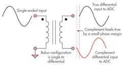
Most high-speed ADCs use a differential input structure, which provides good common-mode noise rejection capability. However, this requires many acquisition systems to convert a single-ended signal into a differential signal at the front of the ADC input. A passive balun or transformer and an active amplifier are the main choices for this single to differential signal conversion process. While there are many high-performance component choices for this part of the system, even the best solutions will embed some small differential imbalances that distort the signal of interest and decrease the SFDR through the ADC.
Phase mismatch between each side of the differential input signal at the front end of the ADC creates an increase in power for the harmonics of the fundamental signal. This can happen when one side of the differential signal leads the other side in time by some amount of phase relative to its period. The effect can be seen in Figure 4, when one side of a differential pair leads the other side by a small margin of periodic phase.
Another imbalance at the front end of a differential signal acquisition system can be amplitude mismatch. When one side of a differential signal has a different gain than its complement, the ADC input sees one side as a larger signal and the other as a smaller signal. This otherwise reduces the full power of the fundamental signal and decreases the SFDR in dBc. A 2-dB amplitude mismatch between differential inputs will result in a 1-dB full-scale reduction in the power of the input signal. Each of these front-end signal integrity issues has the potential to degrade the SFDR of the ADC as well as the signal deciphering capability of the total system.
What are some ADC architectures that could limit SFDR?
Several ADCs that sample up to and beyond 1 GSPS employ an interleaving scheme of a couple or a few discrete channels or cores to achieve the full high-speed data rate. For example, a dual-channel ADC could be used with each core rotating through the sample acquisition process, by use of interleaving, to achieve the full sample rate. While one channel is sampling, the other would still be processing previous samples. Interleaved architectures could also use three or more ADC cores.
Using an interleaving method, multiple ADC cores can work in parallel to achieve a higher sample rate than otherwise could be achieved with a single core. However, slight variances in phase, offset, gain, and bandwidth exist between the inputs of each of these cores. The result is that new interleaving artifacts and image spurs can be introduced into the frequency spectrum, which reduces the wideband SFDR of the ADC. This will diminish the system’s dynamic range and its ability to distinguish a weak signal of interest from the interleaving spurs. To mitigate the artifacts seen from an interleaved ADC, a system engineer may have to read detailed application notes about special calibration modes and methods to plan around the spurs.
A monolithic ADC architecture, in which there is only one processing core, will not exhibit interleaving spurs. A single pipeline core ADC is an example of a wideband converter that will tout a relatively high SFDR, typically limited by the second or third harmonic.
What would the performance of an interleaving ADC look like in the frequency domain?
For a sampling architecture comprising three discrete interleaved cores, there are two gain and phase image spurs and one offset spur (Fig. 5). An offset spur can be seen at 2/3*Nyquist, but is not a dominant contributor to SFDR in this case. SFDR limiting gain and phase spurs are seen at (2/3*Nyquist ± analog input frequency).
The greatest spur in magnitude will be the dominant contributor to the SFDR of the system. Without the interleaving spurs, the SFDR would otherwise be the dynamic range from the fundamental frequency to the second harmonic. The performance penalty in this particular case is a –8-dB reduction in SFDR due to the interleaving image spurs.
For a sampling architecture comprising four discrete interleaved cores, there are three gain and phase image spurs and two offset spurs (Fig. 6). There are offset spurs at Nyquist and ½*Nyquist present and another image spur at (Nyquist – analog input frequency), but these are not the dominant contributors to SFDR in this case. The dominant gain and phase spurs are seen at (½*Nyquist ± analog input frequency).
If these spurs are greater in magnitude than the second or third harmonics, they will be the dominant contributor to the SFDR of the system. Without the interleaving spurs, the SFDR would otherwise be the dynamic range from the fundamental frequency to the third harmonic. The performance penalty in this particular case is a –13-dB reduction in SFDR due to the interleaving image spurs.
Other SFDR Limitations
Another potential area for SFDR degradation is a system design that allows outside noise to couple onto either the analog or clock input of the ADC. Additionally, the digital outputs of an ADC have the potential to couple back to the input if a system board layout is not carefully planned. Outside noise also can couple onto a reference, a supply, or a ground domain of the ADC. If the noise is significant enough and semi-periodic, it can show up in the frequency domain of the system as an unwanted SFDR limiting spur that is unrelated to either the fundamental frequency or the ADC architecture.
The Future of GSPS ADCs
GSPS ADCs that provide a high wideband SFDR, without the interleaving artifacts that have limited system performance in the past, are now available. The AD9860 is a dual-channel, 14b, 1-GSPS ADC that achieves SFDR of 78 dBc with a 1-GHz input. The AD9625 is a 12b, 2-GSPS ADC that offers typical wideband SFDR of 80 dBc with a 1-GHz input.
SFDR is an important and key performance metric in GSPS and ADCs. Wideband SFDR is typically limited by the second or third harmonic of the fundamental signal. Single monolithic pipeline ADCs and other advanced architectures are advancing a new frontier in high-performance GSPS converters. They do not exhibit the interleaving spurs in the frequency domain that have historically been present within ADC architectures in the GSPS space.
For those applications that require a wideband response, it can be problematic to navigate, plan, and remove these artifacts. New solutions solve these system issues to provide state of the art SFDR performance across a wideband spectrum.
References
W. Kester, “Understand SINAD, ENOB, SNR, THD, THD + N, and SFDR so You Don’t Get Lost in the Noise Floor,” MT-003 Tutorial, www.analog.com/static/imported-files/tutorials/MT-003.pdf
M. Looney, “Advanced Digital Post-Processing Techniques Enhance Performance in Time-Interleaved ADC Systems,” Analog Dialogue 37-8, August 2003
W. Kester, Analog-Digital Conversion, Analog Devices, 2004, ISBN 0-916550-27-3, Chapter 6; also available as The Data Conversion Handbook, Elsevier/Newnes, 2005, ISBN 0-7506-7841-0, Chapter 2
W.C. Black Jr. and D.A. Hodges, “Time Interleaved Converter Arrays,” IEEE International Conference on Solid State Circuits, Feb. 1980, pp. 14-15
W.C. Black Jr. and D.A. Hodges, “Time Interleaved Converter Arrays,” IEEE Journal of Solid State Circuits, Dec. 1980, Volume 15, pp. 1022-1029
J. Harris, “The ABCs of interleaved ADCs,” EDN Network, Feb. 17, 2013, www.edn.com/design/analog/4407107/3/The-ABCs-of-interleaved-ADCs
Ian Beavers is an applications engineer for the High Speed A/D Converters team at Analog Devices Inc., Greensboro, N.C. He has worked for the company since 1999. He has more than 18 years of experience in the semiconductor industry. He has a bachelor’s degree in electrical engineering from North Carolina State University and an MBA from the University of North Carolina at Greensboro. He is a member of EngineerZone’s High-Speed ADC Support Community. Feel free to send your questions to IanB on Analog Devices EngineerZone Online Technical Support Community.
About the Author
Ian Beavers
Product Engineering Manager, Automation Energy and Sensors, Analog Devices
Ian Beavers is a product engineering manager for the Automation Energy and Sensors Team located at Analog Devices, Greensboro, N.C. He has worked for the company since 1999. Ian has over 20 years of experience in the semiconductor industry. He earned a bachelor’s degree in electrical engineering from North Carolina State University and an M.B.A. from the University of North Carolina at Greensboro.
Comment About the Article
To join the conversation, and become an exclusive member of Electronic Design, create an account today!

Leaders relevant to this article: