Use Analog Techniques To Measure Capacitance In Capacitive Sensors
Download this article in .PDF format
Capacitive sensors are found in a wide range of equipment, from consumer electronics to industrial/process control. Touch buttons are increasingly found in lamps and dimmers. Motion detectors can detect miniscule changes in deflection. Hygrometers indicate humidity changes. Pressure sensors and accelerometers are moving toward capacitive sensing. And, capacitive displacement sensors are even found in disk drives.
These sensors produce an output: capacitance. Measuring this capacitance is an inherently analog problem that can be very tricky. Often, these sensors provide the most trouble for engineers to interface to microcontrollers. While some microcontrollers offer built-in simple routines for capacitive touch buttons, their measurements are relatively crude and designed for measuring a change in capacitance—useful for detecting a finger placed on a touch sensor, but not for industrial and displacement sensing requiring absolute accuracy.
Capacitive Sensors
As a specific example of a capacitive sensor, consider a capacitive relative humidity (RH) sensor. In this type of sensor, the dielectric material is designed to absorb water vapor from the external environment when exposed. The electrical capacitance increases as the dielectric absorbs water, since the dielectric coefficient increases with increased moisture—a direct indication of the relative humidity. The net dielectric coefficient is also sensitive to temperature variations, so the humidity calculation involves both a measurement of capacitance and temperature.
Humidity sensors exhibit a relatively small change in capacitance over their output range. A capacitance change of 40 to 50 pF over 0% to 100% RH with a 0% RH capacitance (C0RH) of 100 to 200 pF is not uncommon. A typical sensor offering 3% absolute accuracy (with 1% repeatability) corresponds to a resolution requirement of 1.5 pF.
Some capacitive sensors measure displacement. In their simplest form, these sensors are constructed with precision metal plates in close proximity, and an electric field is maintained between them. The resulting output capacitance (usually small, in the 10-pF range) depends widely on the geometry of these sensors.
Timer Approaches
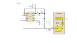
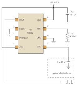
The most common approach to measuring capacitive sensors is simply to use an analog timer circuit to generate a frequency that is inversely proportional to capacitance and then utilize a microcontroller to count pulses within a given period to calculate the frequency (Fig. 1). Thus, there is no requirement for an analog-to-digital converter (ADC) or comparator in the microcontroller. The basic equation relating the measured capacitor C and frequency F is:
F = 1/(C * (R1 + 2 * R2) * ln2)
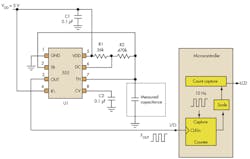
Astable timers, such as the classic 555, operate by charging and discharging a capacitor. The capacitor voltage triggers the charge and discharge cycles as it transitions across a lower and upper threshold. Despite specifications touting higher than 1-MHz operation, typical CMOS 555s “like” to operate in the 5- to 10-kHz range for best accuracy (Fig. 2).
The table shows some basic limitations in these circuits. Error A, the first, shows that a few picofarads of input capacitance exist on the TH and TR pins. Since this is the connection point for the capacitor measured, this parasitic capacitance (along with the stray capacitance shown in row F in the table) adds erroneously to the measured capacitor value. For capacitance measurements above 100 pF, this can be accounted by characterization and subsequent accounting when arriving at the capacitance value. (For lower capacitance values, see the discussion below.)
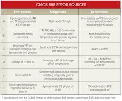
Comparator timing delays and a finite discharge FET on-resistance (B and C, respectively) set the upper frequency bound for operation. Far below these speeds, errors creep in from the variability of these parameters, making them hard to calibrate out. For example, there is a strong temperature dependence for the discharge FET on-resistance and a VDD dependency for comparator delay.
Measuring Low Capacitance Values
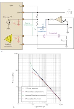
To measure smaller capacitance values, the effects of TH and TR pin input capacitance can be compensated (electronically subtracted). Two methods include passive and active compensation.
Passive compensation involves connecting compensation capacitors to create a charge pump to null the effect of pin input capacitance. The Q (output) pin swings at a higher level than the capacitor voltage ramp, so strapping a capacitor from Q to TH and TR effectively transfers net coulombs into the measured capacitor. As C and Q are inversely related, this equals a negative capacitance, as seen by calculating the total charge Q accumulated on the measured capacitor C for a given charging cycle:
• No compensation:
Q = C * 1/3 * VCC
• With compensation:
Q = (C + Cx) * 1/3 * VCC – CX * VCC
Q = (C -2 * Cx) * 1/3 * VCC
So, to first order, 2 * CX capacitance is subtracted from C (assuming CX << C).
A voltage step will be seen on the measurement capacitor from charge transfer. This doesn’t affect timer operation adversely. It simply shows charge added and subtracted to compensate for the added parasitic pin capacitance. Since capacitance at dc also affects the output, a small capacitor is added there too.
A choice of CX = 4 pF was found empirically to be acceptable. A second capacitor, CY (not shown), was also added to compensate the input capacitance at dc.
Active compensation requires an op amp and can result in a more precise, adjustable compensation. An op amp’s output is connected to the compensation capacitor CX, driving it in concert with the capacitor’s voltage ramp. (Be sure to use a stable op amp driving this capacitance!) By varying the gain G of the op amp, and thus the amplitude of the ramp, you can vary the amount of compensation capacitance to subtract, according to:
Ceq = C – CX(G – 1)
Alternatively, a “hybrid” of passive and active compensation can be implemented, which saves the cost of the op amp while retaining adjustability. A variable amplitude comparator can be utilized, with an adjustment to the amplitude of the square wave made by adjusting the voltage of a linear regulator.
Remote Sensing
Sometimes it’s not possible to co-locate the sensor and the measurement electronics. The capacitance measured can be placed some distance away from the measurement electronics. But unknown capacitances to ground along the wired path of the capacitor will add and subtract from the measured capacitance value in this case, especially if it’s cabled.
The impedances driving the capacitor are generally high (>500 kΩ), and long wire lengths can pick up electric fields and induce spurious voltages (especially from 60-Hz ac mains). Shielding the cable can help, but this naturally creates additional capacitances that vary according to cable length, adding to the capacitance measurement errors.
The solution is an active shield, driven by an op amp to dynamically servo the shield to the same voltage as the capacitor voltage, nulling the capacitance from shield to capacitor voltage. This remote capacitor solution essentially requires three connections: shield, capacitor voltage, and a separate wired ground return. The principle is similar to the active pin capacitance compensation described earlier. The shield can also be driven with a gain slightly higher than 1 to additionally compensate for pin capacitance, though the chosen gain will necessarily need to change with different cable lengths (Fig. 3).
Measurement Speed And Accuracy
The measurement speed of these capacitance-to-frequency systems is determined by the time it takes to count the number of clock cycles corresponding to the capacitance value. Accuracy to first order is determined by the number of cycles counted. Since capacitance is inversely proportional to frequency, given a fixed measurement time, the schemes naturally provide the highest bit resolution for the lowest capacitance values in a given range. This is not necessarily the desired result, since the lowest capacitance values will have the highest analog errors.
Alternatively, utilizing a fast microcontroller clock to determine the timer’s period provides a higher resolution for higher capacitance values. (A 24-MHz system clock can resolve a 14-bit value for 1 kHz, in the 1-nF range.) In some microcontrollers, this higher-frequency clock operates with higher accuracy than the lower-frequency clocks.
Noise in the measurement will likely drive the measurement time and averaging lengths. Frequency noise in the timers is primarily generated by the comparator’s timing jitter. This jitter increases as a percentage as the period frequency decreases, making small capacitor value measurements noisier.
Faster Approaches
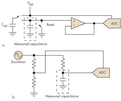
A few other approaches are worth mentioning, some of which yield faster results (Fig. 5).
In the charge-balancing scheme, a reference capacitor is charged to a known voltage and then discharged across the measured capacitor. Besides the problem of providing a reference capacitor, there are two major problems with this method.
First, the switch itself injects charge into the circuit, affecting the result. Even the very best analog switches exhibit at least 1 pC of charge injection, limiting the scheme to higher measured capacitor values. Second, the buffer op amp must have extremely low leakage. For 1-nF capacitor measurement, 10-nA leakage drops the voltage on the measurement capacitor by 1 mV within 100 μs.
Capacitive bridge methods involve injecting a known excitation frequency into a capacitive bridge (often simply an R-C network) and comparing the resulting response with a reference path. A true bridge circuit would involve two R-C arms in the bridge with a nulling scheme utilizing adjustable capacitors.
The reference path here is a simple resistive divider and serves as the reference for a ratiometric ADC measurement, considered a more practical method. The scheme requires a fast ADC to convert the amplitude of the R-C network and to deduce the measured capacitor value. The ADC must be fast, and some signal processing may be involved in the measurement. Extreme care also must be taken to limit the loading (capacitive and resistive) on the measured capacitor.
Op-Amp Integrator Methods
Op-amp integrator-based capacitor measurement schemes drive precision currents into the capacitor, determining capacitance by assessing integration time. A precision resistor (good absolute tolerance is required), an op amp, and potentially a comparator (to turn the integrator into an astable oscillator) are required to generate the measurement current to feed the capacitor. However, some benefits may outweigh the extra components over timer-based systems.
The circuit essentially drives one side of the capacitor while maintaining a virtual ground at the other side. The benefits of a virtual ground are twofold. First, the op amp’s input pin capacitance no longer affects the measurements, since this node remains at ground. Second, the capacitor now can be measured remotely without an actively driven shield (the shield can remain at ground potential), relieving the requirement for an op amp capable of following the timer ramp and driving high capacitance.
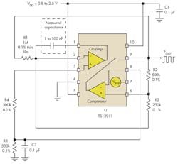
Figure 5 shows an example circuit for this approach, utilizing an op amp and comparator. Here, the op amp is driven in an astable fashion, triggering a hysteretic comparator to switching the polarity at two thresholds. Like the timer circuit, this circuit offers a very simple relationship between C and F:
F = 34 * R1 * C
The Touchstone TS12011 “nanopower” op amp/comparator/reference IC is used here since it offers both a comparator and an op amp in a single package. Additionally, the entire circuit runs at less than 5 μA (from a 1.8-V supply) and can run from supply voltages as low as 1 V. The circuit is best used for measuring capacitances from 1 nF and higher, since the resulting frequency output is well within the bandwidth of the op amp, and the variation in the comparator delays adds a small error to the result.
For lower-value capacitance measurement, a higher-bandwidth op amp would be appropriate, together with a faster comparator. To keep the frequencies relatively low, minimizing timing delay-based errors, low-leakage input op amps such as JFET-input op amps are best.
Conclusion
There are several ways to measure capacitive sensors. With some careful design and in appropriate capacitance ranges, traditional timer circuits may suffice. For low capacitance values and high accuracy, other options such as integrator-based designs may need consideration.
About the Author
Comment About the Article
To join the conversation, and become an exclusive member of Electronic Design, create an account today!

Leaders relevant to this article: