This article is in Bob Pease on Analog Vol. 1 in the Analog section of the Electronic Design Library.
Members can download the PDF ebook.
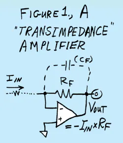
One of the first things you learn about operational amplifiers (op amps) is that the op amp's gain is very high. Now, let's connect a feedback resistor across it, from the output to the -input. When you put some input current into the -input (also known as the summing point), the gain is so high that all of the current must go through the feedback resistor. So, the output will be VOUT = -(IIN × RF). That's neat (Fig 1). While we used to call this a "current-to-voltage converter," which it is indeed, it's also sometimes referred to as a "transimpedance amplifier," where the "gain" or "transimpedance" is equal to RF.There's a whole class of applications in which this configuration is quite useful and important. An important case is when you need an op amp to amplify the signal from a sensor, such as a photodiode. Photodiodes put out current at high impedance (high at dc), but often they have a lot of capacitance. If you just let the photo diode dump its current out into a resistor, there are two problems (Fig 2). If the sense resistor is large, then the gain can be fairly large, but the response will be slow and the time-constant will be large: t = RL × CS. But if you choose a small sense resistor to get a small t, the gain will be low. The signal-to-noise ratio (SNR) may also be unacceptable. How can you avoid poor gain and/or poor response? Kay garney? (That's Nepali for "What to do?")
To avoid this terrible compromise, it's a good idea to feed the photodiode's output current directly into the summing point of a transimpedance amplifier(Fig 3). Here, the response time is not RF × CS, but considerably faster. Plus, the gain can be considerably larger, because now you can use a larger RF. This helps improve the signal-to-noise ratio too!
When you connect up the diode like this, the first thing you realize is that the darned thing is oscillating! Why? Well, it's well known that the input capacitance of an op amp (and its circuitry) can cause instability when the op amp is used with a feedback resistor. You usually need to add a feedback capacitor across RF to make it stable. In the old days, it was stated that:
CF × RF = CIN × RIN
So if you have a unity-gain inverter with RIN = RF = 1 MO, and the input capacitance of the op amp is 10 pF, then you're supposed to install a feedback capacitor of 10 pF. That's what people said for years. The LF156 data sheet stated this, and it still does. But that's not exactly true. A complete explanation is a bit beyond the scope of this column, but in practice you can usually get away with a much smaller feedback capacitor. In many cases, you can get a response that's improved by a factor of five or 10, and still not get excessive (more than 5% or 10%) overshoot. In practice, you have to tweak and optimize the feedback capacitance as you observe the response.
The formula for the optimized amount of CF is, if:
then:
but if:
the feedback capacitor CF should be:
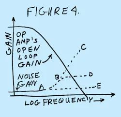
Now, whenever you have an op amp with a large CS, a large RF, and a small CF, the noise gain will rise at moderate frequencies. The definition of noise gain is the reciprocal of the attenuation from the output back to the -input. In other words, if the attenuation is ZIN/(ZIN + ZF), then the noise gain is 1 + ZF/ZIN.
At moderate frequencies, the ZF is determined by RF, and ZIN is established by CS. So, the noise gain will rise until the frequency where the impedance of CF becomes equal to RF. Then the noise gain flattens out, typically at a large number, such as 20, 40, or 80. We do this because if the noise gain kept rising at 6 dB/octave while the op amp's gain is rolling off at 6 dB/octave, the loop is going to be unstable, and it will oscillate. The reason that we choose a small value of CF is to make the noise gain flatten out, make the loop stable, and stop the oscillation and ringing (Fig. 4).
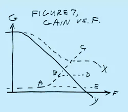
If you make CF = CIN, you can get the noise-gain curve to stay flat as in line A-E. It will be very stable but have a very slow response. If you add no feedback capacitor, the noise gain will tend to rise as per line A-B-C. This will cause instability. Selecting a suitable small value for CF can get the smooth results shown by line A-B-D. Yeah, it's as easy as ABD to get fast, stable response by picking a small CF. So, we have made the feedback capacitance big enough to stop the oscillation and minimize the overshoot. Now what?
There's a pretty good book by Jerald Graeme (ex-Burr-Brown) on the topic of the transconductance amplifier: Photodiode Amplifiers—Op Amp Solutions. Jerry and I have definitely come to the same basic conclusion. When you want to optimize a transimpedance amplifier, everything interacts. Therefore, every time you compute the response and the noise, and change any factor, the computations may change considerably. There's no simple or obvious way to compute or optimize the performance. The performance, in terms of response or bandwidth, in terms of peaking or overshoot, and in terms of noise or SNR, is an extremely complicated, nonlinear, and highly interacting function of:
- the feedback resistor
- the source capacitance
- the feedback capacitance
- the desired bandwidth
- the desired gain factor (which does predict the full-scale output voltage)
- the voltage noise of the op amp
- the current noise of the op amp
- the input capacitances of the op amp
- and the gain-bandwidth product of the op amp.
Jerry and I certainly agree on that. Jerry's book is well written, and for just $55, it's pretty much a bargain. I recommend it: ISBN = 0-07-024237-X.
But I also have worked on this general problem many times over the years and have several suggestions that go be-yond Jerry's book. More on this later.
There are several basic rules of thumb that Jerry and I agree upon:
(A) You want to avoid an op amp with high voltage noise (nV/vHz).
(B) You want to avoid an op amp with high current noise (pA/vHz). (Most bipolar op amps have much higher current noise than FETs.) It's a rare case when an op amp with bipolar input transistors is better, except when RS is very low or resistive (or in cases where the input is capacitive but the bandwidth is narrow).
(C) You usually want to avoid an op amp with large input capacitance. Unfortunately, most data sheets don't properly specify the op amp's input capacitances, neither differential-mode nor common-mode. But it's fair to assume that most "low-noise" op amps have a larger input capacitance than ordinary op amps. You may want to ask the manufacturer, or you might just decide to measure it yourself.
(D) Much of the noise of such a transimpedance amplifier is proportional to vBW &215; CSOURCE × VN of the op amp. So if you want to get low noise, you must optimize very carefully. Specifically, begin by computing the im-pedance ZS of your sensor at the maximum frequency of interest:
ZS = 1/2pFCS
For a good amplifier, the voltage noise and the current noise times ZS should both be as small as you can get. If one of these noises is much larger than the other, then you're probably far off optimum.
(E) If you have any choice of what sensor you employ, try to find a lower-capacitance sensor. Furthermore, make a low-capacitance layout between the sensor and the op amp.
If you want to get fast response, low noise, or wide bandwidth, Jerry's book offers some pretty good advice. More on that later.
But Jerry didn't include a list of good op amps that have low voltage noise, and/or low current noise, and/or low input capacitance. Because some are better than others, I bet you can use Paul Grohe's selector guide to find some low-noise op amps. See www.national.com/selguide for free "Selguide" software that can run on your PC to help you select a good, low-noise, inexpensive op amp.
Also, Jerry neglected to mention that you can design your own op amp with better, lower voltage noise and better bandwidth. I mean, op amps that you can buy off the shelf cover a wide array of cases where they are optimized for low VNOISE and low INOISE, wide bandwidth, low power drain, and so on. But you can "roll your own" surprisingly easily and accomplish even better performance for a specified application! I'm not proposing that you design a complete op amp, but it's simple to just add a new low-noise front end ahead of a suitable op amp.
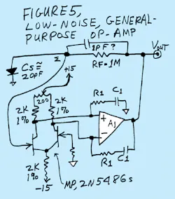
The basic idea is to add a couple of good low-noise FETs in front of an existing op amp. Most op amps don't operate the front-end transistors as rich as the output. Yet in a case like this, there's no reason at all not to run more current through the front end than in the rest of the op amp. My first pick is the 2N5486, which has less than 1 pf of CRSS, but has a lot of gms (4 millimhos) and low voltage noise (at IS = 3 mA). So for my first design, I'll just put a matched pair* of 2N5486s in front of a decent wideband op amp, such as the LM6171(Fig. 5). What's the voltage noise of this amplifier? We may be able to get an average of 3 nV/vHz, out to 10 kHz.
When you're designing an op amp, remember this: adding gain is one of the cheapest things you can add. You on-ly need to be careful about how to give that gain away—to roll it off.
In this case, it's easy. The R1-C1 network in Figure 5 just rolls off the gain for a fairly smooth frequency response. To achieve 2 MHz of bandwidth and a fairly good, smooth 6-dB/octave rolloff, I suggest R1 = 75 O, and C1 = 100 pF as a good place to start your design.
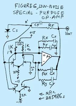
But now, look at the refinements in Figure 6. We can roll off the amplifier's gain simply in two swoops. The low-frequency gain is rolled off by RX and CX. Then after the gain rolls off flatly, we roll it off some more by RY and CY. When we are finished, it should look something like curve X in Figure 7. This isn't exactly rocket science. We just want to make it a practical design. But this is a whole system design. You can't very well design and optimize the op amp alone. It's the op amp, the feedback system, the noise filters, and the post-amplifiers that have to be considered and optimized all together.
My first-hack proposals for these damping/stabilization components are:
RX = 5.1 kO, CX = 50 pF
RY = 330 O, CY = 7.5 pF
The whole point behind making your own op amp is that you do not have to just build an op amp with a smooth 6-dB/octave rolloff, all the way out to a few megahertz. You can roll off the gain at a 6 dB/octave out to some intermediate frequency, and then flatten out the gain. Then, at a higher frequency, let it roll off some more in some vaguely controlled way. This would make a lousy general-purpose op amp, but it might be ideal for a case where the noise gain is rising, such as in a transimpedance amplifier. (Look at the old LM709. When you choose the correct damping networks, it can provide a gain of 1000 out to some high frequency like 1 MHz.)
Also note that I added a second pair of 2N5486s to improve the voltage noise. Yes, this will approximately double the input capacitance. But if your CS is already large, this may easily improve the signal-to-noise ratio. If it's good to have two, will three be better? I'll let you figure that out! But, yes, four or five may provide definite improvements... or that might not be the case.
I won't recommend that you design your own op amp if you can buy one that does the job. But if the best one you can buy isn't good enough, then there's some hope here. Designing your own composite op amp is not that hard, and not that expensive, even if you are going to build one or 10 or 1000. The post-amplifier can be inexpensive. Of course, all of the basic designs will be somewhat different if you are running on ±5-V supplies, or ±15-V supplies.
Either way, it's not that difficult, but the design compromises are slightly different. Here, I just showed a couple of ±15-V applications. (The ±5-V designs differ mostly by using a low-voltage, rail-to-rail-output op amp.)
In future columns on this topic, I will comment on other aspects of design and optimization for transimpedance amplifiers.
Meanwhile, try to avoid Tee networks in the feedback network. They often cause poor signal-to-noise ratios. Next time, I'll explain that completely. Yes, a Tee network might help you avoid buying 1000-MO resistors, but that's only okay when you have proven that the noise is okay.
All for now. / Comments invited!
RAP / Robert A. Pease / Engineer
Read more article from Bob Pease on Analog Vol. 1.
*For this case, grade a good number of 2N5486s into 20-mV bins of VS, with VGD = 7 V, and IS = 3.8 mA. Take units out of the same bin for good matched pairs.
P.S. If you design in an op amp, try to avoid relying on nonguaranteed characteristics, such as noise, which is rarely guaranteed.
P.P.S. I neglected to mention that any resistor may have a built-in capacitance of 0.3 to 0.8 pF. If you add that to any imperfect layout, the capacitance could be so big that you wish it were smaller. Good layout and good engineering can easily cut the C to less than 0.2 pf. For example, make the feedback resistance out of three or four resistors in series, and install a shield land between the ends of the resistor. More later. /rap
About the Author

Bob Pease
Bob obtained a BSEE from MIT in 1961 and was a staff scientist at National Semiconductor Corp., Santa Clara, CA, for many years. He was a well known and long time contributing editor to Electronic Design.
We also have a number of PDF eBooks by Bob that members can download from the Electronic Design Members Library.
Voice Your Opinion!
To join the conversation, and become an exclusive member of Electronic Design, create an account today!

Leaders relevant to this article:

