The Flash Memory Summit continues to be the place where the latest storage technology is announced. This year is no different with a host of new approaches to storage in addition to ever-increasing capacities. On the horizon is quad-level cell (QLC) flash memory that stores four bits of information in a single cell. This extends the current crop of SLC, MLC, and TLC flash memory technologies.
There were impressive multilayer solutions like 64-layer NAND from Toshiba, Western Digital, and Micron. These build on the 32- and 48-layer NAND implementations from previous years. The latest implementations can pack 4 Tbytes onto a single M.2 module. Intel’s XPoint memory will be highlighted at this year’s Intel Developers Forum, which is just after the Flash Memory Summit.
There were a couple of other technologies that stood out that would be of special interest to embedded developers. Everspin is delivering its 256 Mbit DDR3 chips based on its perpendicular magnetic tunnel junction (pMTJ) ST-MRAM. MRAM is faster than flash memory and does not suffer from a limited write lifetime. This is one reason that Diskfull Writes Per Day (DWPD) is a common specification for solid-state drives (SSDs).
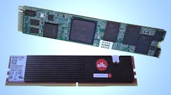
Aupera’s Aup-AXL-M128 M.2 module (Fig. 1) uses Everspin’s new MRAM chip. The M.2 module is delivering four orders of magnitude BER reduction. It also uses 30% less power. Everspin also demonstrated an NVMe board using its chip that delivered 1.5 million write IOPS. Controllers can be simpler than their flash-memory counterparts because MRAM does not require wear leveling.
Another switch from the conventional flash-storage methodologies was from Diablo Technologies, which is now shipping its 256 Gbyte Memory 1 DIMM (Fig. 2). This 256 Gbyte flash memory module fits in a DDR4 slot, but it is not destined as non-volatile storage when mixed with Diablo’s DMX software. Instead, the combination is taking advantage of flash memory’s higher density and lower cost compared to DRAM.
A typical server would fill its memory slots with a combination of DDR4 DRAM and Memory 1 modules, usually with more Memory 1 modules. This allows up to 2 Tbytes of storage on the processor’s memory channel, but it will not be accessed like DRAM. Instead, it acts as a second-level cache. The DMX software hooks into Linux’s virtual memory support and moves data to Memory 1 as it becomes mostly read-only. This is typical for a large number of most applications like database servers. Data that is updated frequently remains in DRAM and cached data is brought back into DRAM as needed.
Storage is getting increasingly complex. Processors typically have a few cache levels. This adds another for main memory, and larger server farms typically have more for SSDs and disk drives. Even those have caching internally. On the plus side, most of this is transparent to developers and their applications.


