We’ve all experienced the effect of electrostatic discharge at some point in our lives, the most common case being a tingling sensation one feels after touching a door knob or any metal surface. When the body is electrically isolated from earth, like with a pair of rubber sandals, a few foot slides can make it charged. This charge is maintained until the body comes in contact or in close proximity with a conductor that serves as a discharge path.
If the body would feel a jolt, the electromotive potential induced is in the order of 4 kV. Although, 4 kV sounds like a scary figure, the body’s resistance is fortunately within the megohm range. Thus, the effective power isn’t enough to cause any internal injury.
I remember trying to measure my body’s resistance waaaaay back when I was in college, during a laboratory class. I was goofing around, wondering what the multimeter would read when I placed the terminals in between the palms of my hands, and I indeed got unstable readings in the hundreds of kilohms and megohm range. Unsatisfied with my foolishness, I tried placing the terminals between the ends of my forehead (in an attempt to measure the resistance of my brain), but the readings remained the same. I finally stopped when my colleagues started giving me queer looks. Hmmm.
Anyway, this same phenomenon does not only vex the lay man but the design engineer too. Over the decades, a variety of methods have been tested and implemented to mitigate the consequences of ESD (more on these later). The need to regulate these effects is reflected by the passing of MIL-STD-1686 (to my surprise, these four numbers matched my employee ID, what are the odds?), created by the U.S. Department of Defense aimed at minimizing effects of ESD on parts, assemblies, and equipment through a control program.
We are also concerned with MIL-STD-750 and MIL-STD-883, where various test methods and models are defined for semiconductors. Document copies of these standards are publicly available through MIT. I went through them and fell asleep maybe after the 400th page or so. After a few more pages, I finally found the section of interest at page 512—method 3015.7 “Electrostatic Discharge Sensitivity Classification,” which occupied a modest five pages out of a 700-page PDF file.
How ESD Affects Semiconductor Devices and Circuits
Before delving into complex testing procedures, it would help intuition to know what’s happening when semiconductors are subjected to ESD. The manufacture of semiconductor circuits not only involves components that were intentionally made, but also those that come as a consequence of the circuit’s construction and architecture.
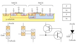
These parasitic components play crucial roles in circuit design and analysis, and usually effectuate the malfunction of an IC. Some examples would be the parasitic capacitances between junctions that form an electrical short to high-frequency components and the parasitic thyristors between transistors that form an electrical short when activated. Figure 1 shows one such parasitic thyristor in an inverter configuration.
It is worth noting that the parasitic transistors, which form a parasitic thyristor, have very low current gains and can’t be turned on by very short pulses, such as line reflections on the circuit board (they exhibit a comparatively low transit frequency). However, ESD that lasts even for a few tens of nanoseconds can trigger the entire parasitic thyristor due to a flooding of charge carriers. In earlier generations of CMOS circuits, a simple rapid rise in the supply voltage would be a sufficient trigger condition. The thyristor will also latch when the IC is subjected to a high source of ionizing radiation.
Latch-up in a parasitic thyristor can be prevented by increasing the distance between components. Doing this reduces both current gain and triggering sensitivity. However, there’s a tradeoff between the maximum distance between components and the need to design transistors with characteristics similar to each other (because transistors in current mirrors and differential pairs need to be identical for ideal current “mirroring”). Another workaround is to add guard rings to critical parts of a circuit.
Standardized ESD Models Used by Industry
Many established models can test the reliability of semiconductor circuits and devices against ESD. In this section, I will just mention a few of the most popular ones. Perhaps the most pervasive are the human-body model, the machine model, and the charged-device model.
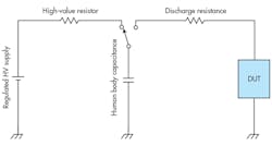
The human-body model is, as the name implies, a model for simulating the ESD of a human being that takes a path from the finger through the DUT and then to ground. Figure 2 shows the human-body-model test circuit.
The capacitor in the test circuit is charged by a high-voltage supply through a high-value resistor. The standard supply voltage is ±2 kV, the high-value resistance at 1 to 10 Mâ¦, and the capacitance at 100 pF (with 10% tolerance and 1012 minimum insulation resistance). A high-voltage relay breaks the connection to the supply and creates a path for discharge to the DUT. The discharge resistance, representing the resistance from the metal contact to the DUT, is at 1.5 k⦠(with 1% tolerance).
These are just common values, though. In reality, the human body’s capacitance swings from 150 to 500 pF (affected by contact area and shoe size). Also, the discharge path should be characterized by a lower resistance given that metallic conductors are the more common medium. These inconsistencies are addressed by Standard IEC 802-2, recommending a capacitance of 150 pF and a discharge resistance of 330 â¦. However, this standard doesn’t directly involve integrated circuits.
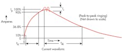
The definition for the impressed current waveform is also stringent for the human-body model (Fig. 3).
A rise time of less than 10 ns should be satisfied with a peak current not exceeding 10% of the corresponding stepping current (please see the copy of the standard for more details). This definition is of major interest because ESD protection circuits aren’t instantaneously driven to conduction and require a certain amount of delay also in the order of a few nanoseconds.
If you’re looking for a testing method with higher peak current levels, a faster rise time, and more voltage spikes (than what’s offered by the human-body model), then IEC 61000-4-2 provides just that. It does so because it’s designed for testing in an end-user environment. Some ESD protection mechanisms are placed in integrated circuits just to survive the assembly and integration process toward a finished product. IEC61000-4-2 takes the testing to the next level by ensuring that the finished products will survive ESD under normal operation.
Another ESD model, the machine model, has been downgraded by three standards bodies and is no longer a requirement in the automotive industry. However, some are still using this model, so it’s worth mentioning here.
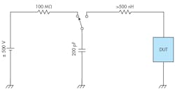
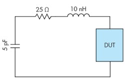
The machine model is used to simulate discharge from moving insulators [usually plastic bearings] within machinery or other similar equipment. Figure 4 shows the model’s test circuit.
The configuration is similar to the HBM except for the discharge resistor, which was replaced by an inductor. This is because charged metal parts in machines have very low resistances. A well-known consequence of not having a discharge resistor is uncontrolled current (aside from those that function as bleeder resistors perhaps?). No control over current transients results in unknown rise times that allow bypass of ESD protection and destruction of the DUT (at voltages near 500 V). This is one reason why the machine model has lost its popularity.
Lastly, the charged-device model arises due to ESD during PCB mounting of the integrated circuit. It took a tedious investigation to prove this phenomenon, where the integrated circuit gains charge as it slides along the plastic rails of the production line and discharges upon touchdown on the PCB. The equivalent circuit for this model is shown in Figure 5.
The values for the capacitance and inductance are quite small since ICs, like the best things in life, come in small packages. The setup is quite complex, so a summary is well in order. The flat side of the DUT is laid on a metal plate, with its pins facing upward. The DUT is then charged using a moving test probe through the pins and discharged with a second test probe. Studies show that if the DUT survives a charging voltage of around 1 kV after discharge, then the probability of failure in the assembly line is infinitesimal. Studies also show that there is no correlation between results from the charged device model tests and the human-body-model and machine-model tests. I have no means of proving the claims of these studies and the source is obscure so don’t take my word for those last 2 sentences.
Protection Against the Adverse Effects of ESD
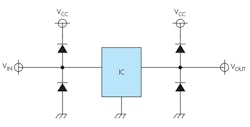
Depending on the application, an ESD protection circuit can be designed in many ways. Common sense dictates placing such protection in parallel with the DUT rather than in series. One common technique is to employ shunt clamping diodes. The diode’s fast switching action, as well as the simplicity and economy of the circuit, are attractive. Figure 6 illustrates a common implementation of ESD diodes at the terminals of an IC.
ESD diodes are internal. The upper diode is forward-biased when VIN is greater than VCC plus the diode’s threshold voltage, while the lower diode is forward-biased when VIN is more negative than the negative of the diode’s threshold voltage.
The lower diode also prevents a short between the input and the collector/drain of the first input transistor (usually connected to VCC). This happens because the upper parasitic transistor discussed earlier is no longer in cutoff. That’s why in most datasheets, you will see the range of the allowed negative input voltage to be only around –0.3 to –1 V. (This used to puzzle me, too—why can I bias the input at significant positive magnitudes, but not at a mere –0.7 V? The analysis above enlightened me.)
These ESD diodes also serve a bonus function. They can be used to subject the DUT at a more accurate temperature in the absence of a type T thermocouple by utilizing the trend of their threshold voltage with respect to temperature.
Problems arise when the ESD diode’s slew rate doesn’t meet the rise time of the ESD pulse. In effect, the diode doesn’t turn on. When it does, heat from conducting diodes can damage adjacent components (higher-frequency components contain higher energies). Also, such diodes may break down under high-voltage ESD transients. Such hazards call for extra measures like adding a second-stage ESD protection circuit (Fig. 7).
In this two-stage ESD protection circuit, there are two transistors that help short the positive high-voltage ESD transient to ground, while the diodes take care of negative excursions. The MOS helps drive the base current of the PNP transistor at even higher magnitudes of positive voltage.
The above circuits are for internal implementation. There are also external circuits designed for extreme cases, such as nuclear EMPs from detonated atom bombs above the atmosphere and lightning EMPs from lightning strikes during a thunderstorm. In these circuits, transient-voltage-suppression (TVS) diodes and buffers (having internal ESD diodes themselves) are implemented with additional stages included. The working principle is similar to the ESD diode discussion above, except now the diodes have higher power ratings as the stages go outward. For a three-stage external ESD protection circuit, one can expect voltage limiters that carry currents in the range of hundreds of amps, followed by transient voltage suppressors, then ordinary ESD diodes, all connected to earth ground.
You may be asking, can’t we use transistors as the limiting components of an ESD protection circuit? I have come by that kind of circuit, which was designed by Texas Instruments. The company constructed it for applications that can’t wait for the input voltage to exceed VCC plus the threshold voltage (the chip may operate abnormally at, like, VCC + 0.1 V or VCC + 0.05 V, as in high-precision op amps).
Do-it-Yourself ESD Testing Techniques
(Warning: This section is written as a spoof, so the author has no claims on the effectiveness and safety of the methods described below.)
Who needs to shell out money for an ESD gun or an MK ESD automatic tester to test your product against ESD? With these nifty techniques, you won’t have to spend a dime (because these methods are downright straightforward).
1. Walking on a carpet method
For this, you’ll need your living-room carpet, some rubber sandals, and yourself. Place the DUT on a flat table. Settle yourself in an upright standing position on the carpet. Slide your left/right foot, then the next, following a circular path. After skidding 50 times, quickly touch the pins of your DUT on the table. Take some anti-dizziness pills and check if the DUT is still working. Kudos if your IC hasn’t been damaged.
2. Dancing on a carpet method
This is a variation of the first method, which is more enjoyable in my opinion because it doesn’t make you giddy. Ever wanted to dance to some music on rubber sandals? In this method, you can work while grooving to your favorite songs. Just replace the 50 skids in the previous methods with a dance to a song. My choice selections are “What Does the Fox Say?” and “Macarena.” For experienced users of this method, I highly recommend Michael Jackson’s “Thriller” and MC Hammer’s “You Can’t Touch This,” guaranteed to ensure your IC’s immunity to ESD. Kudos if your IC hasn’t been damaged yet.
3. The balloon and comb method
Purchase a rubber balloon for birthdays (a hot-air balloon, too, if possible; we’ll need it for the next method), a vanity mirror, and a plastic comb if you don’t have one. Sit yourself comfortably in front of the board and DUT. Comb your hair while looking in the vanity mirror then smile. After admiring your gorgeous self, set the cracked mirror aside and start rubbing the comb on the balloon, maybe a hundred slides will do. Comb the pins of your DUT afterwards, and then check if it is still working. Kudos if your IC hasn’t been damaged.
4. The Thor method (Warning: extreme caution advised)
This method, in spite of having some hazards and limitations, is a favorite of mine because it absolutely guarantees that your IC is really ESD-proof. I haven’t had an IC that was tested with this method ever fail from ESD! Sadly, it can only be done during a thunderstorm (or when you are feeling really really lucky). If you observe nimbus clouds in the sky, head for the nearest open field with your board and DUT. Don’t forget to bring a bucket of saltwater and a hot-air balloon (optional).
Upon arrival, locate yourself to the middle of the open field and pour the bucket of saltwater over you and your board (you can remove your clothes if you want to keep them dry). Firmly hold the board in your hands and put it overhead. Wait until lightning strikes the board. When it does, rush back to your testbench and check if the DUT is still working. Kudos if your IC hasn’t been damaged.
If you have been waiting for an insufferably long time, the hot-air balloon then comes in handy. Pour salt water over you, the board, and the balloon. Pump up the balloon with hot air and ride it to the dark cloudy skies. Hold out the board and wait until it gets struck by lightning. Jump off the balloon and rush back to your testbench. Check if the DUT is still working. Kudos if your IC hasn’t been damaged.
Develop Better ESD Models and Improve ESD Protection Circuits
The burden on ESD testing may be lessened if we continue developing devices that counteract ESD. Reflecting on the matter, what else can we do? It’s interesting to brainstorm on solutions to these kinds of problems. Anything we come up with can also serve as stepping stones to other solutions.
I once had an idea of using a small strip of wire located near the power-line interface to detect huge voltage anomalies before they enter the IC terminals, though there’s the problem of latency. Can you think of any possible solutions that can help in our fight against ESD?

