The Dark Force Of Evil In Electronics: Electromagnetic Interference
Is there an electronic product or circuit that’s not susceptible to electromagnetic interference (EMI)? For that matter, are any devices EMI-free? Simply put, no. EEs wish it wasn’t the case, of course, but it’s a fact of life in electrical engineering— and it’s one of those things they typically don’t teach you in school.
Most engineers find out about EMI on the job, where expunging it often takes more time than the original design itself. And don’t forget that federal and international regulations mandate EMI control according to a wide range of rules. This requires the testing and certification of any equipment before it can be sold.
EMI DEFINED EMI is the general term used for electrical signals that interfere with the normal operation of electronic equipment. All electric and electronic systems and equipment generate some kind of signal that could potentially interfere with the normal operation of another nearby piece of equipment.Also, EMI can degrade the performance of equipment, introduce errors or operational faults, or cause complete failure. It may be self-generated, where one circuit interferes with another inside the equipment, or externally generated by some other device or equipment within the same environment.
The earliest form of EMI, radio-frequency interference (RFI), consisted mainly of harmonics and spurious signals from radio transmitters that interfered with other radios. For example, ham and citizen’s band radios generated harmonics that produced television interference (TVI).
We’re expected to see an exponential rise in EMI due to the growing number of wireless devices and standards, including cell phones, Wi-Fi, Bluetooth, ZigBee, WiMAX, and GPS. While RF sources still cause interference, digital equipment and computers have become the preeminent cause of EMI. The very high clock speeds with fast rise and fall times cause digital signals to generate huge bandwidths of large harmonics.
Switch-mode power supplies also generate EMI. Increased use of microwave frequencies for radio as well as digital applications has produced even more EMI. What was once a relatively minimal problem has turned into a challenge for most design engineers.
Electromagnetic compatibility (EMC) occurs when a piece of equipment can operate normally in an environment with other electrical and electronic equipment. With EMC, the equipment won’t generate EMI, nor is it susceptible to EMI from another source in the operating environment. The goal is to eliminate EMI or greatly suppress it to avoid interference and achieve EMC.
Still, questions and concerns abound. Can your TV operate without interference from a nearby PC? Will your security system be compromised by radiation from some nearby RF source? Can your garage door be opened by the harmonics of a passing two-way radio transmitter? Will your DSL interfere with your telephone operation? Does your cell phone really interfere with the navigation or landing systems on an airliner?
Can radios operate reliably in an environment where every piece of equipment has some electronics? How do you keep all the radios inside a cell phone from interfering with one another? Recently, while filming some videos at a conference, I experienced one of the many kinds of EMI when two other nearby wireless microphones interfered with my microphone. And just imagine the EMC issues experienced on the battlefield. Will radar systems interfere with one another or missile systems or satellites or vice versa?
TYPES AND SOURCES OF EMI The two main types of EMI are conducted and radiated. Conducted EMI is noise or interference that’s passed over wires and cables from a source or emitter to the receiver or “victim” device. The most common conducted path is via power lines. The ac lines are a major source of EMI because of spikes and noise generated by a wide range of devices connected to the line. Motors and switching sources are the main examples.Then there are the signals that leak out of a power supply on to the ac line to be passed along to another device connected to the ac line. Power connections from power supplies to circuits are other sources. A huge amount of conducted EMI is passed through poor grounds.
Radiated EMI is the wireless transmission of signals from source to victim. Capacitive and inductive coupling from one circuit to another is one type of radiated EMI. This type of coupling is often called near-field interference. One example is crosstalk from one wire to another in a cable. All closed-loop circuits carrying current generate a magnetic field that can potentially induce a voltage into an adjacent circuit.
Far-field interference is the reception of electromagnetic or radio waves. A radio wave is a combination of a magnetic field (H) plane at a right angle to an electric field (E) plane. Both travel perpendicular to those planes. These fields behave as James Clerk Maxwell explained them back in the 19th century.
As the waves travel together, the magnetic field recreates the electric field and vice versa. The far field begins approximately at a distance beyond ?/2p meters. For example, one wavelength is 30 cm at 1 GHz. Therefore, the far field begins at about 30/6.28 = 4.78 cm from the source and beyond. Inside that range is the near field, which consists mainly of a predominant magnetic or electric field.
Any kind of noise is also a form of EMI. Noise is either external or internal. Manmade noise, coming from sources like fluorescent lights and auto ignitions, is the worst type of external noise. Spikes on the ac line caused by switching loads such as motors, contactors, or relays off and on are instances.
Even the electric and magnetic fields produced by the 60-Hz line itself are a major EMI headache for some types of equipment that process weak medical and audio signals. Other external noise sources are atmospheric noise from lightning and extraterrestrial noise from sources like sunspots or the aurora borealis.
Internal noise, e.g., thermal and semiconductor noise, is less of a problem. The one exception involves very small signal applications, especially in RF front ends. EMI may also come from intermodulation distortion (IMD), where two internal signals mix in some nonlinear device or circuit to produce sum and difference frequencies and other combinations with harmonics. These are especially hard to overcome.
Don’t forget electrostatic discharge (ESD) as an interfering source. ESD, of course, is the momentary current flow that occurs when a high voltage between two points is dissipated. Lightning is the most powerful example, but any static discharge can produce EMI and damage unprotected circuits.
Finally, you can categorize EMI as either narrowband or broadband. Narrowband EMI usually comes from a single sinewave source or one that’s modulated over a limited channel, such as radio and TV transmitters, cell phones, and other radios.
A broadband source produces a wide swath of harmonics. Any electrical disturbance (switching spikes on a power line, for instance) is an example. Also, any highspeed digital source is considered broadband. Other common broadband sources include computers, embedded controllers, and switching power supplies.
MITIGATING EMI EMI management spans a huge range of solutions at both the emitter and victim devices. Some can be as simple as increasing the spacing between the source and the victim. Or, maybe even physical orientation can solve the problem—for instance, by rotating one device 90° or rerouting cables. However, the real solution involves proper design of all equipment to minimize emissions or to make the equipment less vulnerable to external EMI. Three different methods help reduce EMI: filtering, shielding, and grounding.One direct way to eliminate unwanted signals is by filtering them out. Passive filters work well, and they are widely used in most new equipment to minimize EMI. It usually starts with an ac line filter that keeps bad signals from getting into the power supply and the powered circuits and keeps internal signals from being added to the ac line.
These shielded low-pass filters are almost standard in every ac-operated device today. There are two sections: one for common-mode interference and the other for differential-mode interference. Both types of interference occur in most equipment (see “Understanding Common- Mode And Differential-Mode Interference”).
Bypassing and decoupling for all circuits is essential. In most designs today, every IC must have its own decoupling with low- Z capacitors and sometimes with accompanying resistors or inductors. Ceramic capacitors in the 0.01- to 0.1-µF range are best and must be connected as close to the IC pin as possible. Any low-Q plastic or electrolytic capacitors obviously need to be further bypassed with a ceramic capacitor to ensure full filtering.
Filtering is commonly added to cables and connectors on lines into and out of a circuit. One solution is low-pass feedthrough capacitors with integral inductors or ferrite cores that attenuate the signals. Some special connectors also have built-in low-pass filters. Such low-pass filters “soften” digital waveforms to increase rise and fall times to reduce harmonic generation. Occasionally, a series resistor working with some stray or distributed capacitance is adequate for this purpose.
Adding filters to critical circuits is also prudent. Transmitters should have a lowpass output filter that attenuates harmonics if the LC matching network at the output doesn’t perform this adequately. Input filters on RF receivers can also help eliminate unwanted signals. A 60-Hz notch filter may be needed to get rid of pesky 60-Hz “hum” in medical or audio equipment.
Common-mode signals picked up on a cable by radiation or via inductive or capacitive coupling can be eliminated by wrapping several turns of the cable around a ferrite rod or toroidal core. Special split cores are used to simplify this implementation. This approach is widely used with PC cables for video and on some ac lines.
Shielding is the preferred way to contain any radiation or coupling in source or victim devices. It usually involves encasing the circuit inside a completely sealed metallic box or other enclosure. For most products, this becomes inconvenient and expensive. However, it may be the only effective way to control EMI and meet the necessary regulations.
Shielding reflects electromagnetic waves back into the enclosure. The shield absorbs the waves that aren’t reflected. In most cases, a small amount of radiation penetrates the shield if it isn’t thick enough.
Almost any common metal like aluminum, copper, or steel makes a good shield. For plastic enclosures, a metallic material may be sprayed or otherwise deposited on the plastic material to provide adequate shielding. At lower frequencies, the shield doesn’t always have to be solid. Screen materials or perforated metal works as well and also provides ventilation, which is often a problem with solid shields.
The main problem with shields is the leakage that occurs from seams and openings. Seams are areas where two metallic surfaces come together. Openings are almost always needed to accommodate cables and connectors. These openings and gaps in the seams act as antennas and cause radiation to escape.
Any opening about the size of one quarter to one half wavelength of the main signal frequency will act like a very efficient slot antenna. As a result, any gaps or openings must be as small as possible. Generally, openings and gaps should be no more than 1/20th of a wavelength for commercial equipment and less than 1/50th of a wavelength for military equipment.
To solve the seam leakage problem, the two mating surfaces should be clean and highly conductive as well as extremely flat. In addition, fasteners like screws attaching a cover plate to a box shield should be placed as closely together as possible to reduce gap size. This is often a major nuisance, so gaskets can be used to fill the gaps. A wide range of special conductive and flexible gasket materials is available for almost any shielding need.
While simple in concept, grounding is a black art in electronics. What you assume to be a “good” ground often isn’t. The ground, of course, is that magical common connecting point that provides a reference for most signal and supply voltages. The problem is that grounds aren’t perfect.
Instead of having zero impedance between any two points on the ground, there is some resistance and inductance. This impedance forms a ground loop. Multiple currents flowing between these two points produce a voltage. This noise voltage is a form of EMI that’s particularly hard to eliminate except through good initial design.
At low frequencies—audio and below— grounds are less critical. Heavy wire, a wide copper path on a printed-circuit board (PCB), or even a metal chassis is typically okay. But once you move into the higher RF and microwave frequencies, extreme measures are needed to get a good low ground impedance.
RF grounds and digital grounds are often large copper ground planes within a PCB. These large areas of copper have very low impedance. Multiple ground points across the board are the best way to achieve low-Z grounds and minimal ground voltage. To achieve the best ground:
• Use multiple grounding points on a large ground plane for best results.
• Keep any leads from ICs or other components to ground as short as possible to reduce the inductance.
• Isolate circuits from ground if ground loop voltages can’t be controlled any other way. For example, use a transformer, common-mode choke, or optical isolators to separate grounding points from circuit inputs and outputs.
• Maintain separate grounds for digital and analog circuits and then combine them later at a single point.
• Separate grounds for I/O circuits, which often have higher currents, are sometimes necessary to solve a ground loop problem.
Single-point grounds are great for lowfrequency systems, but not so much for high frequencies. Connections to that single point may be too long and could add inductance and resistance.
PCB LAYOUT Smaller circuits and higher frequencies have forced PCBs to be smaller and, as a result, harder to design. Smaller boards make it more difficult to predict where EMI will occur or become a factor. Today, board layout is a major project, representing a significant chunk of the design costs. A few guidelines do apply, though.First, unless it’s a simpler design, use a multilayer board. It’s difficult to lay out and more expensive to make, but a multilayer board is the one element you can adopt to minimize EMI in almost any product. Power distribution is handled with large ground planes that reduce ground impedance and provide integral power bypassing via the interlayer capacitance. Multiple power distribution buses can keep sensitive circuits isolated from one another.
Next, pay attention to clock frequency and distribution. Clocks are major EMI generators, so their lines must be carefully routed to prevent high-speed signals from being driven into sensitive circuits. Start by using the lowest possible clock frequency. Keep all clock lines as short as practical. If clock drivers are necessary, make sure they are no faster than necessary.
Add series resistors into clock lines to lengthen rise/fall times. Also, don’t forget that using spread-spectrum clocks can greatly diminish EMI for some applications. The spread-spectrum clock modulates the clock frequency over a narrow range and spreads the clock signal over a wider bandwidth but significantly reduces the amplitude of the frequency components.
Third, when laying out any circuit, keep in mind that the current loop of any circuit will radiate differential-mode EMI. This radiation in terms of field strength voltage is directly proportional to the current (I), the area of the loop (A), and the square of the frequency (f ), or V ˜ I × A × f2/r, where r is the distance from the loop. Also, don’t let copper traces cross over any gaps or openings in the ground return plane. These gaps act as efficient antennas and are a major contributor to EMI.
Finally, use a PCB layout program that’s EMI-aware. As part of the company’s Expedition PCB layout tool, Mentor Graphics’ Quiet Expert (QE) employs rules instead of simulation to identify problems and suggest fixes.
CABLES Cables are huge sources of EMI—they act as antennas and radiate an enormous amount of interfering signals. The connectors that attach to the cables are just as guilty. So, use shielded cables to minimize EMI. Coax is preferred, because it’s essentially self-shielding. The shielding usually extends through the connector.Unshielded twisted pair (UTP) is a widely used cable. The twists help the magnetic fields produced by each wire cancel one another, reducing radiation. The UTP is still subject to crosstalk from stray capacitive coupling, though. Adding a shield to the twisted pair makes it almost as good as coax. The shield is grounded, and the location of that ground can affect the shielding effectiveness.
I/O connections can sometimes be made with special shielded connectors. Be on the lookout for the many available versions of these special connectors. Also, power wiring is harder to protect, so keep it short and bypassed. Use feedthrough capacitor/ low-pass filters where possible to keep out the bad signals.
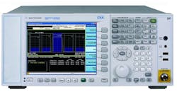
TESTING AND TROUBLESHOOTINGSome EMI can be tracked with a standard oscilloscope that has sufficient bandwidth. But scopes don’t show the whole picture. Here, a good spectrum analyzer is needed, one with a bandwidth beyond what your harmonics and spurious signals may occupy. Signal analyzers like Agilent’s X-Series (EXA/MXA) are designed for EMC testing (see the figure).

The antenna is often mounted on a non-conducting tripod, and the equipment under test (EUT) is placed on a rotating table. The measurement is field strength in V/m or dBµV/m. An antenna factor derived from the antenna in use is applied to the analyzer reading to get a direct measurement in dBµV/m. Special probes detect near-field magnetic and electric fields at close range. These help you track leakage at package seams and openings, as well as cable radiation.
You also will need a line impedance stabilization network (LISN) for conducted EMI. This standardized low-pass filter is inserted between the ac power line and the EUT to keep any power-line EMI from entering the EUT or to minimize any EUT-generated EMI from getting to the ac line. The LISN also has a circuit that will pick off any EMI generated by the EUT and send it to the analyzer input.
There are two basic rules for EMI testing. First, test often. Initial testing can come during initial breadboarding, then PCB layout testing, prototype evaluation, and in final production. Second, be sure you know the standards to which you are testing—that is, know your regulatory objectives (see “EMI/ EMC Regulations”). The Federal Communications Commission (FCC) rules typically state specifically what the test setup and parameters are for compliance.
About the Author
Staff
Articles, galleries, and recent work by members of Electronic Design's editorial staff.
Comment About the Article
To join the conversation, and become an exclusive member of Electronic Design, create an account today!

Leaders relevant to this article: