NFC/RFID Ripe for Application Expansion
Near-field communications (NFC), previously considered merely the next generation of barcodes, has proven to be much more than practical and robust. New applications have moved beyond traditional simple, intuitive, safe, contactless transactions to an array of new applications driven by unconventional thinking.
At the physical or RF layer, NFC is still essentially an evolved form of RFID. In fact, NFC was built over the 13.56-MHz (HF) RFID. The NFC Forum, an industry consortium, 1 started with the RFID physical-layer protocol and added a few new layers to the protocol stack. Then the NFC Data Exchange Format (NDEF) was put in place to identify, encapsulate, and exchange application data between NFC-enabled devices.
Readers and Tags
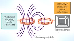
NFC/RFID works over a distance of a few inches up to a meter. The technology leverages inductive coupling to transfer energy through a shared magnetic field between two devices. Essentially, the reader’s antenna coil is the primary and the tag’s antenna coil is the secondary.
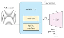
When placing a tag in close proximity to the reader, the field from the reader’s antenna coil couples to the tag’s antenna coil. A voltage is induced in the tag, which is then rectified and used to power the tag’s internal circuitry. The reader modulates the field to communicate its data with the tag (Fig. 1).
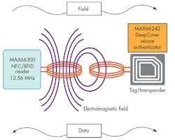
Figure 1 is an example of a passive tag that doesn’t need an external energy source to function. Instead, a passive tag obtains its energy from the reader’s electromagnetic field. Typical applications include access control, smart posters, loyalty cards and coupons, mobile payments (contactless credit cards), ticketing, and transportation toll collection.
Beyond that, with passive authentication, designers can now collect and exchange secure system configuration and calibration data with portable electronic products, even when the portable device has lost its main power source or isn’t operational. The solution in Figure 1 allows any embedded electronic product to interface wirelessly with any surrounding devices and networks over its I2C interface.
More Advanced Security
Security is essential for wireless NFC/RFID applications. One way to achieve that is to integrate advanced security into the passive tag authenticator, which combines a wireless NFC/RFID interface with an I2C interface, data-protection modes, fast data transfer; and energy harvesting in the tag. NFC/RFID operates at a carrier frequency of 13.56 MHz, which is part of the globally available and unlicensed radio frequency ISM band. The technology has a few existing released standard specifications, including ISO/IEC 14443 Types A&B, and ISO/IEC 15693.2
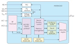
Such security is the bailiwick of the MAX66242 (shown in Figure 1), which integrates SHA-256 crypto engine that provides a symmetric challenge-and-response authentication capability based on a shared secret key (Fig. 2). A 32-byte SRAM buffer facilitates fast data transactions over the I2C interface.
This file type includes high resolution graphics and schematics when applicable.
Energy Harvesting, Added Flexibility and Scalability
Energy harvesting is very useful because it makes the MAX66242 a flexible and scalable solution for a wide range of NFC/RFID applications.
As a generic passive tag, the IC doesn’t require an external power source. It only needs a very small amount of power to operate—around 50 µA or slightly more depending on the features supported. The tag extracts all of its energy from the reader’s 13.56-MHz HF electromagnetic field. When the antennae have been constructed correctly and tuned for an efficient and optimized link, this passive tag gets much more energy than is necessary to power itself. The leftover energy is often shunted to ground.
The rectifier’s unused harvested energy in the MAX66242, on the other hand, is collected and sent out of the IC through its VOUT pin. This harvested power can now be used to power surrounding ICs in an application such as the temperature-sensor patch, from which temperature conversion data is also collected. The IC’s VOUT pin can be configured to provide either 1.8 or 3.3 V (typical). This configurable supply output can deliver up to 5 mA, given adequate field strength.
Enabling NFC/RFID in a Portable Device
It’s fair to say that NFC/RFID is currently making a grand entrance in the consumer wearables technology mass market. Operating under the banner of the Internet of Things (IoT), more sensor-enabled embedded systems will be designed and set up to collect user-biometric and other data from multiple device systems on a network. Scads of NFC/RFID-enabled medical and industrial applications are anticipated, and we have yet to see the limits.
A basic circuit architecture that will enable NFC/RFID in an embedded design can be achieved with the MAX66242 (note that the system needs a communication path to the outside world) (Fig. 3).
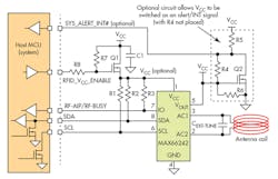
In the figure, while the I2C interface (SDL and SDA) and the PIO signals (a multiplexed line of the RF-AIP and RF-BUSY functions) are necessary to connect to the host microcontroller, the RFID_VCC_ENABLE and SYS_ALERT_INT# signals are optional. The MOSFET Q1 is utilized for isolation. Since the tag’s internal EEPROM is accessible through both the RF and I2C interfaces, Q1 powers the tag when the host microcontroller must interface with it in the absence of an HF field. The optional Q2, however, is used to switch the open-drain SYS_ALERT_INT# with a regulated VCC on the board. (R4 is not placed in this case.)
With a variant of this proposed circuit block implemented in the device schematics, the OEM’s product is ready to communicate with any NFC/RFID reader or initiator system. Once the board enters an HF field, VOUT comes up and turns on Q2. The open-drain signal SYS_ALERT_INT# goes to low, which interrupts or wakes up the host microcontroller, thereby indicating that the system is in an HF field. The host microcontroller then drives the RFID_VCC_ENABLE into a logic-high state, switching the MOSFET Q1 on. The host microcontroller is now ready to exchange data bytes with the NFC/RFID reader device that supplied the HF field.
Again, the VCC pin of the MAX66242 doesn’t need to be connected to power, as the IC’s internal circuit is powered from the energy harvested from the HF field. However, the VCC pin is left connected so that the host microcontroller can access the IC in the absence of an HF field.
Developing New Applications
As mentioned, NFC/RFID promises to empower new potential usages in the industrial and medical sectors. A partial list of these new applications includes automated device configuration (also known as behavior setting), usage limit setting, system alert setting (e.g., system wakeup), slave-device secure authentication, and sensor-tag implementation, just to name a few.
One particular emerging growth area for NFC/RFID is the sensor tag. A sensor tag is an assembly (e.g., a patch) that contains a sensor IC to monitor defined physical parameters from the users’ behavior and the surrounding environment (Fig. 4). This sensing operation occurs along with the tag’s normal identification function.
An attractive feature of a secure sensor tag is its ability to collect and report physical parameter measurements without a wired connection. In this case, the example MAX66242 is the key component for a sensor-tag discrete implementation.
Medical consumable applications of a sensor tag include the temperature patch and the sun-protection-factor (SPF) patch. Once a patient is fitted with the disposable temperature-sensor tag patch, the nurse can take core body temperature measurements without physically touching the patient. Given the global concerns about hidden and dangerous viruses, this offers a healthy way to mitigate or completely eliminate cross-contamination situations in a hospital or medical clinic.
In the same manner, an SFP sensor-tag patch can help a beachgoer apply the correct sunscreen lotion to avoid sunburn. The user would only need to read the SPF patch occasionally with a smartphone.
A sensor tag can also help monitor the integrity of a shipment. For example, a shock or vibration sensor tag will provide evidence of shock during the transportation of a valuable and/or fragile item.
In such an application, the MAX66242’s master I2C port is a key differentiating feature. If there were no master I2C port, the design would need a small microcontroller to collect the temperature conversion data, and then write this data into the tag’s memory for collection later by the reader (Fig. 4).
As was mentioned earlier, the sensor tag transforms (or transduces) physical analog quantities into digital outputs. Here, the NFC device is essentially the bridge or conduit connecting these outside analog parameters to useful information that the user can read on the screen of a smartphones or tablet. Again, no external energy source is needed with a sensor tag using this design, because it uses its energy-harvesting VOUT pin as a power source for the sensor IC.
Diagnostics/Error Data Collection
A design such as that in Figure 4 literally enables any embedded system to communicate with NFC-enabled portable communication devices. The NFC/RFID port can also represent a warning display to the service technician similar to the service-engine-soon light seen on a car’s dashboard.
After implementing the above circuit architecture in any embedded design, the system can now exchange wireless information with the outside world, including diagnostics and error codes, data gathered from failing circuits, runtime warnings, and other system configuration/commissioning and calibration data. All of this flexibility allows an OEM to add even more value-added features to its end products.
It’s even possible to store system runtime vital diagnostics and error data. Such data could be uploaded later after the system is “dead” or not powered. The collection of this system health and faults data is done over the NFC/RFID tag’s interface (Fig. 5).

During normal system operation, certain vital operating parameters of each point-of-load (PoL) regulator are continuously monitored. While in this constant monitoring mode, the system manager can also perform corrective measures in response to faults or operational warnings.
It’s even possible to create a “message-in-the-bottle” or “black-box flight recorder” scenario where the vital out-of-range parameters can be stored (e.g., the parameters of trip points from all of the monitored fault protections circuits). Using the RFID/NFC reader, the technician now has access to the deregulation measurements recorded just instants prior to the actual failures.
Such data can also be used later to predict certain specific faults as well as help recognize abnormal operating conditions much earlier than before. This added intelligence about faults would help predict, mitigate, or even eliminate certain root causes of known catastrophic failures with next-generation products.
An NFC/RFID application in industrial control and automation can be found with field sensors and I/O cards. The MAX66242 tag allows for the commissioning of the sensor card while the device is sitting unpowered on the shelves. Analog calibration data, key parameters, or other system-level information is downloaded into the tag on the sensor or I/O card using a smartphone just before it is installed. Thus, consumers can use their smartphones to buy credits for certain devices and use the smartphone application (app) to load the credits or enable the feature via the portable device’s NFC/RFID connection.
This file type includes high resolution graphics and schematics when applicable.
References:
1. For more information, go to http://nfc-forum.org/.
2. These specifications are in an ISO Standard document. They are known but not freely available on the Internet. One must pay to receive a copy. For more information, go to http://www.ansi.org/.
Hamed M. Sanogo, executive business manager at Maxim Integrated Products, is responsible for the Secure Authenticator and NFC/RFID product lines. Hamed graduated from the University of Alabama at Birmingham (UAB) with a BSEE, and earned an MSEE at the University of Michigan-Dearborn and an MBA in Technology Management at the University of Dallas. Hamed can be reached at [email protected].
