Advanced Smart Sensor Networks Open Up A Multitude Of Applications
We’re awash in a world of sensor components that can measure and, with actuators, act upon any sensing function imaginable. These include acceleration, gyroscopics, magnetic headings, sound, video, pressure temperature, liquid and gas flow, motion, humidity, light, and many other natural functions in gas, liquid, and solid media. Many of these sensors are microelectromechanical systems (MEMS).
Related Articles
- Wireless VIbration Sensors Enable Continuous And Reliable Monitoring
- Energy Harvesting Powers Wireless Sensor Networks In Industrial Apps
- Power Your Wireless Sensors For 40 Years
Much of the buzz about sensors involves the onslaught of smartphones, which portend a rising tide of applications that will transform our lives. Yet these sensors also herald oncoming applications in medical, industrial, military, automotive, intelligent building, infrastructure monitoring, geophysical exploration, agricultural management, natural-disaster monitoring, climate change, energy harvesting, and myriad other fields whose proofs of concept have already been demonstrated.
Smartphones and tablets are the largest sensor drivers for the fast-growing consumer electronics market, which market analysts expect to grow to about tens of billions of dollars within the next few years, paced by the use of combo sensors that include an accelerometer, a gyroscope, and a magnetometer. But that will pale once billions and trillions of sensors find use across other industries.
Expert Opinions
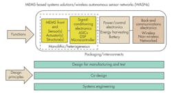
A sensor is a fundamental link between the world and how electronics technology reacts to its inputs. It vastly differs from other components like resistors, capacitors, inductors, and LEDs, notwithstanding their beneficial impact on society. As such, sensor devices must be considered a vital part of a smart sensory system that integrates sensors, actuators, and other structures with other functionalities like signal processing, power, control, and networking, all delivered in a package optimized for specific applications. This has important ramifications for design principles like co-design, systems engineering, design for manufacturing, packaging, and testing (Fig. 1).
The systems engineering concept is an important point that many experts on MEMS/actuators and non-MEMS devices have been stressing for many years. It is becoming even more relevant with the advent of smartphone platforms, wireless communications, cloud computing, and the Internet, capable of connecting us to many applications.
“It has become a necessity for suppliers of sensors to embrace a systems approach for the design and manufacture of products that best meet their customers’ needs,” says Roger Grace, president of Roger Grace Associates, a marketing consultancy that has specialized in sensors for over 30 years. “As the sensor elements become more mature and evolve into commodity items, suppliers must find ways to effectively differentiate their product offerings. They’re providing the customer with a complete solution/one-stop one-shop approach to solving their application using integrated MEMS/sensor-based system solutions (MBSS), where the sensor and signal-conditioning electronics are integrated in one package. This concept is gaining significant acceptance in the market.”
Under the direction of Professor (Emeritus) Kensall Wise, the University of Michigan introduced this concept over 15 years ago and set up the successful Wireless Integrated Microsystems Center (WIMS). The work WIMS is doing in advancing the design, fabrication, and breadth of micro-sensor-driven applications includes advanced materials, processing, biomedical, environmental and structural monitoring, wireless interfacing, and RF MEMS.
Professor Thomas Gessner of Germany’s Fraunhofer Institute in Chemnitz has been a major evangelizer of this approach. Gessner, director of Fraunhofer’s Institute for Electronic Nanosystems (ENAS), created the Smart Systems Integration Conference to share advances of this MBSS concept with its yearly conference attendees (www.smartsystemsintegration.com). This year’s conference will be held in Vienna, Austria on March 26-27.
Speaking at the first Trillion Sensor (TSensor) Summit at Stanford University in California last October, Janusz Bryzek, entrepreneur of many startups and vice president of technology development at Fairchild Semiconductor, as well as founder of the summit, predicted a future market comprising a trillion smart sensors (TSensors) in which every facet of our lives will be affected positively.
Professor Steven Walsh of the University of New Mexico is teaming up with Bryzek to develop a roadmap for the TSensor Summit. Walsh is the co-director of the university’s Technology Management Center and founder and past president of the Micro and Nanotechnology Commercialization and Education Foundation (MANCEF), as well as a leading expert on MEMS business aspects.
“The TSensor market could be the biggest business in the history of electronics,” says Bryzek, driven by the Internet of Things (IoT) and the Internet of Everything (IoE). He cited figures from giant firms like General Electric (GE) and Cisco Systems in projecting a $15 trillion market by 2020. A second TSensor Summit was held at the University of California at Berkeley, and a third took place in Tokyo in February.
Bryzek says that global tides, somewhat overlapping, are driving the demand for smart sensor systems. These include the IoT, which is connecting devices around us through new network architectures to enable low latency control, wearable computing leading to digital health monitoring and wellness, and remote and low-cost medical care. Another tide is the exploding demand for mobile devices transitioning into an “unpad” world of essentially unpackaged communications, computation, and storage “cyber-interface” nodes all interconnected in a vast manner.
The unpad term was coined at U.C. Berkeley’s Wireless Research Center (BWRC). Professor Jan M. Rabaey, the center’s co-director as well as the director of the university’s Multiscale Systems Research Center (MuSyC), envisions a world of TeraSwarm wireless sensor dust nodes, which he described in a presentation at the first TSensor Summit. The open shared platform avoids the present “stove-piping” of sensor nets. The swarm’s cyber-interface nodes all would be interconnected in a vast global network that could cover anything from input/sensory to output/actionary devices that interface the physical and biological worlds with the cyber world.
Bryzek also cites the work that Intel is exploring on context computing to derive information about us and around us and about our feelings, HP’s CEntral Nervous System for the Earth (CENSE) for global environmental monitoring, and IBM’s efforts to give computers five senses in five years as drivers for a TSensor world (Fig. 2).

There are some challenges about the need to be successful to meet the needs of a trillion-sensor market given present technology capabilities. Walsh believes that today’s semiconductor platforms are not scalable and sustainable to support the trillion-sensor solution of the future, yet he is confident that new technologies and materials being developed will be the solution.
Walsh points out that two complimentary and enabling technologies are required for success: data-transmission and storage technology, and data processing technology (i.e., Big Data). He says the rule of thumb in the sensor industry is a system price of at least 10 times the cost of the device, or about $10 per sensor system, considering the gross domestic product (GDP) and workforce numbers, worldwide.
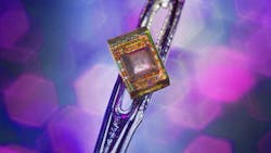
The effort to integrate more functions on a silicon chip in a smaller area continues unabated. MEMSIC, for example, has developed a unique thermal sensing technology that uses heated gas molecules to detect acceleration. MEMSIC’s monolithic MSC6226Xc two-axis accelerometer is based on this technology. It is made on a 0.18-µm standard CMOS process that integrates the sensor elements and its signal conditioning electronics on a single chip. Wafer-level packaging allows the sensor to fit within a miniature 1.2- by 1.7- by 1.00-mm package. The chip is used in many smartphones (Fig. 3). MEMSIC also is planning to announce in the near future a monolithic three-axis version of this chip measuring 1.2 by 1.77 mm. This suits it well for wearable electronics, as well IoT and IoE applications.

“We must have a single smart chip, with on-board intelligence, to serve future large-scale applications and we’re heavily focused on this effort,” said MEMSIC founder, president, and CEO Yang Zhao.
Many semiconductor sensor IC suppliers are not standing still for the future and are preparing for it. But they’re also availing themselves of applications that take advantage of what’s currently available off the shelf. STMicroelectronics has teamed up with Omron Corp. to develop more intelligent MEMS-based gas sensing. They offer what they call a unique gas sensor with built-in correction circuitry for different gas compositions
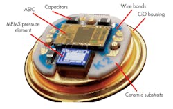
Common sensing applications like pipeline monitoring, process automation, and automotive applications where harsh and caustic environments exist require a systems approach for an advanced and rugged package for developing a suitable sensor/transmitter housing. Keller-Druck’s the Chip-in-Oil (CiO) technology involves a hermetically sealed housing that contains a MEMS pressure sensor from Merit Sensors, an ASIC, and capacitors, all fully immersed in silicone oil (Fig. 4). The MEMS sensor’s seamless integration into an OEM’s product allows for cost savings and system performance not possible with conventional sensing technologies.
Infrastructure Monitoring
The infrastructure in the U.S. badly needs health monitoring and maintenance. Bridges, tunnels, dams, and roadways are monitored by systems using off-the-shelf sensory components and communications systems. Two research centers, the University of Illinois at Urbana Champaign and the University of Michigan in Ann Arbor, have demonstrated leading-edge structural analysis work on bridges.
The research is rapidly advancing the state-of-art in wireless sensors, which are considerably cheaper than wired sensors and offer on-board computing for sensor-based data processing. Research areas include chip stacking, energy harvesting, low-power CMOS circuitry, and wireless transmitters. Current sensors available for installation on bridges are expensive due in part to the need to install wires between sensors. A low-cost alternative to tethered sensors is needed to advance the commercial use of structural health monitoring.
Professor Bill Spencer, director of the Smart Structures Technology Laboratory in the University of Illinois’ Civil Engineering department, is arguably the world’s foremost expert in wireless smart sensing of infrastructure and the use of computerized sensors connected in networks to monitor structural health. Using off-the-shelf components from MEMSIC, he developed the world’s largest deployment of a structural monitoring system for the Jindo Bridge in South Korea.
Professor Gerry Lynch, associate professor at the University of Michigan’s Department of Civil and Environmental Engineering, is exploring wireless sensors for bridge health monitoring using off-the-shelf accelerometers and strain gauges. He has validated his approach on two bridges, the Carquiez bridge in northern California and another bridge in Ypsilanti, Mich.
Lynch pioneered the field of wireless sensors with Narada, a low-cost wireless sensor designed for installation in civil structures. He and his students are collaborating with researchers at KAIST to validate the performance of the sensors on bridges in South Korea. In addition, embedded data processing algorithms are being adopted for automated data interrogation when the wireless sensors are installed on the bridges.
More embedded functions on a chip and the IoT are gaining traction for sensor/actuator, data-storage, data-communications, computer, and software companies. They’re making this investment to prepare for the demands of a future of trillion-sensor world. The Machine Cloud 6.6 developer’s workbench from Axeda Corp., a provider of cloud-based services for building and deploying machine-to-machine and IoT solutions, provides a new user-interface framework, a software development kit for remote access, improved asset search, and analytics and reporting.
Computing, Communications, And Manufacturing Paradigm Shifts
To support this exploding use of sensors, industry is realizing that present computer technology is poorly matched to handle large amounts of data like images and understand them. Major computer manufacturers and other companies are investing more in quantum computing and other methods. For example, Google has teamed up with the National Aeronautics and Space Administration (NASA) to open up a quantum computing lab. They’re using computers supplied by Canada’s D-Wave.
IBM and other companies have made major investments in neuromorphic computing, which involves processing data in a manner similar to the way human brains do. For certain tasks, neuromorphic processors can be more powerful and more efficient than conventional processors. IBM has already released a programming language for neuromorphic processors. Also, Qualcomm has unveiled a neuromorphic program involving tests on a trainable robot.
Google’s Glass with its spectacle-style computing is becoming more embedded in its users’ lives. Mary Lou Jepsen, who works on display technology at Google, has described wearing Glass as “a way of amplifying you.” Georgia Institute of Technology professor Thad Starner, a technical leader on the Glass project, says that the device offers a “killer existence.”
Communications technology also needs revamping. Though U.C. Berkeley’s Rabaey believes that the economies of scale do not yet exist for practical, cost-effective, low-power, self-contained TerraSwarm wireless communications, progress portends possible solutions. Stephan Guttowski, head of the Department of System Design & Integration at the German Fraunhofer Institute, has reported a record small, low-power wireless sensor node Fraunhofer developed that’s a mere 6 by 6 by 6 mm, small enough to easily fit on a single Euro cent, and weighing just 1 gram.
The present method of manufacturing silicon ICs via photolithography may not be sufficient to support a large number of applications in a trillion-sensor world. Printed electronics, which refers to organic or plastic electronics where inks composed of carbon-based compounds are deposited on flexible substrates, appears to be the answer. Printed electronics allow for low-cost volume fabrication with line widths of tens of nanometers or less. This in turn enables even more sensing applications. Research in this field is moving forward. Two such major efforts are underway at the University of Massachusetts at Amherst and U.C. Berkeley.
Another aspect of printed electronics is 3D printing, which produces conductive thermoplastic composites on unmodified commercial systems. Speaking at the first TSensor Summit, Sean Stetson, technical program leader for Motorola Mobility’s Advanced Technology Projects, showed that 3D printing is growing.
Stetson pointed out that product/services revenue from finished 3D printed parts increased in the market from 3.9% in 2003 to 24% in 2011. He also noted that 3D printing allows for the use of piezo-resistive and capacitive electronic sensors, which enables the creation of custom sensing/user interface devices and objects with embedded sensing capability. These include aerosol jets, antennas, interconnects, and sensors on complex geometries.
Still, packaging technology must undergo vast improvements to meet future infrastructure monitoring needs. The University of Michigan’s WIMS center pioneered tiny M3 micromote small form-factor (about 2 mm2) wireless sensor platforms for just such a purpose (Fig. 5).

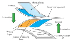
Hughes Metras, vice president of strategic partnerships for North America at France’s CEA-LETI research facility, talked about making arrays of heterogeneous sensors for monitoring large-scale infrastructures. He showed how printed electronics can be laid down on flexible foil substrates that house the sensing, signal-processing, power management, antenna, communications, and solar-powered battery circuitry on multiple foils (Fig. 6).
Smart Roadways, Buildings, and Agriculture
Sensor technology is becoming an integral part of smart and “greener” energy-efficient buildings, driven by the need to reduce energy consumption, costs, and carbon-dioxide emissions. Advances in sensor technology will surely benefit these applications. The sensors will allow demand-based control of lighting, heating, air-conditioning, and ventilation.
Work underway on smart roadway transportation has been proven successful with using the smallest possible sensory component modules, and it may well yet avail itself of much tinier sensor systems in the future. Sensys Networks has demonstrated that “hockey puck” packaged wireless sensor systems just 4 by 4 by 3 in. can be successful when embedded in the roadbed of a highway to detect vehicles. It uses off-the-shelf magnetic sensors and a high level of proprietary software algorithms.
The company is developing a module with high-sensitivity accelerometers to measure roadway vibrations. Its products offer many benefits over conventional loop systems and can be applied to highway vehicle density, vehicle intersection monitoring, pedestrian crosswalk monitoring and control, and parking applications.
The Nest learning home thermostat represents a milestone in home and building automation—so much so that Google purchased the company early this year to build on its commitment to its IoT and IoE efforts. The thermostat’s self-learning algorithm adapts to the user’s setting habits. It is Wi-Fi enabled and can sense near and far motion, ambient light, humidity, and, of course, temperature.
Agriculture is ready to take on even more sensing functions to manage crop growth, harvesting, shipping, storage, and transportation and to make everything more efficient. Agriculture is one of the most important and vital industries on the globe, feeding over 7 billion people worldwide, a population that’s rapidly growing.
Unfortunately, crops are subject to the whims of nature, which are largely unpredictable. NASA and the National Atmospheric and Oceanic Administration are helping to build a precision agriculture approach using GPS sensors, satellites, and wireless communications, benefitting farmers directly.
When you think of a giant agricultural equipment manufacturer like John Deere & Company, you don’t normally think of high technology. But that’s exactly what the company is doing with an R&D group that’s looking to make billions of farm equipment smarter and more efficient, provide better fertilizers, improve irrigation techniques, and provide bioengineering services for the agricultural community of millions of machines and farms and billions of agronomic zones.
“We generated a five- to ten-fold improvement in farm output per hour worked in the 20th century,” says James Linz, information technology manager at John Deere, “and are striving to do more with new technology.” He cites just one example of a sensor-laden combiner/harvester as the next level of controls needed for sensor “perception” to assist or replace the operator (Fig. 7).

So get ready for a smart sensor world in which billions and trillions of smart sensor systems will be upon us in a few more years. The applications they will open up can go as far as one’s imagination, and they will definitely transform our everyday life.
Acknowledgements
The author would like to think the many sensor industry giants, experts, and visionaries who helped him make this article possible. He also greatly appreciates many inputs he received from the visionary organizer of the first TSensor Summit, Janusz Bryzek (more such Summits to follow), and all those associated with that meeting.
About the Author
Roger Allan
Roger Allan is an electronics journalism veteran, and served as Electronic Design's Executive Editor for 15 of those years. He has covered just about every technology beat from semiconductors, components, packaging and power devices, to communications, test and measurement, automotive electronics, robotics, medical electronics, military electronics, robotics, and industrial electronics. His specialties include MEMS and nanoelectronics technologies. He is a contributor to the McGraw Hill Annual Encyclopedia of Science and Technology. He is also a Life Senior Member of the IEEE and holds a BSEE from New York University's School of Engineering and Science. Roger has worked for major electronics magazines besides Electronic Design, including the IEEE Spectrum, Electronics, EDN, Electronic Products, and the British New Scientist. He also has working experience in the electronics industry as a design engineer in filters, power supplies and control systems.
After his retirement from Electronic Design Magazine, He has been extensively contributing articles for Penton’s Electronic Design, Power Electronics Technology, Energy Efficiency and Technology (EE&T) and Microwaves RF Magazine, covering all of the aforementioned electronics segments as well as energy efficiency, harvesting and related technologies. He has also contributed articles to other electronics technology magazines worldwide.
He is a “jack of all trades and a master in leading-edge technologies” like MEMS, nanolectronics, autonomous vehicles, artificial intelligence, military electronics, biometrics, implantable medical devices, and energy harvesting and related technologies.
Comment About the Article
To join the conversation, and become an exclusive member of Electronic Design, create an account today!

Leaders relevant to this article: