This file type includes high resolution graphics and schematics.
Microelectromechanical-systems (MEMS) designers are getting ready for the future as MEMS ICs proliferate across many disciplines and new applications loom. The industry is feverishly improving its processing, packaging, assembly, testing, and hardware and software designs to meet more demanding applications in the industrial, consumer electronics, automotive, medical and biomedical, building automation, and geophysical fields.
Now In Development
To prepare for the next generation of MEMS devices, STMicroelectronics is working with research partners on a pilot line for 200-mm wafers under a project funded in part by European taxpayers. The 30-month, $36 million LabMEMS project seeks to augment MEMS wafer fabrication with magnetic and piezoelectric materials as well as 3D packaging. It will eventually move to 300-mm wafers.
Magnetic and piezoelectric materials form the basis of advanced energy harvesting techniques that are gaining prominence in industrial and medical applications. The project will develop packaging technologies using flip-chip, through-silicon via (TSV), and through-mold via technologies, enabling the development of 3D integrated devices. The research aims to perfect a lead-zirconate-titinate (PZT) deposition process compatible with mass production and integrate it into established MEMS processes.
Related Articles
- Biomedical Devices Improve And Extend Patient Lives
- Energy Harvesting Powers Industrial Wireless Sensor Networks
- Is 3D IC Packaging Ready For Prime Time?
Researchers expect the development of innovative sensors, actuators, micro-pumps, and energy harvesters in system-on-chip (SoC) products that can meet the demands of future data-storage, ink-jet, healthcare, automotive, industrial-control, smart-building, and consumer electronics applications like smart phones and navigation devices. Piezoelectric and magnetic power sources are key elements in low-power energy harvesting technologies.
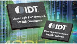
Last year, Integrated Device Technology (IDT) introduced a piezoelectric MEMS resonator that does not use crystals and enables the production of high-performance MEMS oscillators. Its low-voltage positive emitter-coupled logic (LVPECL) 625-MHz CrystalFree pMEMS oscillators feature phase jitter well below 1 ps that suits high-performance communications, cloud computing, consumer, and industrial applications (Fig. 1).
STMicroelectronics and Invensense have made an inertial MEMS sensor available on multi-project wafers for development. Also, X-FAB is beginning production for a first lead customer of a product based on its open platform for three-axis accelerometers and gyroscopes that gives those MEMS chip makers more control in-house using their own ASICs or packaging technology.
An advanced initiative for MEMS ink-jet-based printing technologies is underway by Silex Microsystems, which has joined the European Nanoelectronics Initiative Advisory Council (ENIAC) project known as Processes for MEMS by Inkjet Enhanced Technologies (PROMINENT). It leverages the proven benefits of inkjet technologies to enable higher manufacturing efficiencies, increased production innovation, faster time-to-market, and lower costs throughout the entire manufacturing process. Silex’s contributions include low-cost technologies for low-cost through-wafer vias, hermetic high-vacuum seals for wafer-to-wafer bonding including material deposition, advances in piezo-MEMS fabrication, and other functional materials processing.
Wafer-level packaging and 3D integration are two rapidly emerging trends in MEMS technology where the focus is on developing CMOS-compatible processes for monolithic integration using low-temperature wafer bonding and integrating external passive inductor, capacitor, and resistor elements. Another trend is die stacking in low-cost leadless packages to minimize chip size and meet smaller footprint requirements.
Using silicon interposers to interconnect vertically two or more die stacked in a 2.5D and 3D configuration is a major wafer-level packaging (WLP) challenge that is under intense investigation. Ultimately, the silicon chip may very well serve as the package itself, using metal pads for post-fabrication testing and application.
Sencio BV’s nCapsulate freeform packaging approach offers complete freedom of shape for MEMS devices and cuts down on system assembly costs. The packaging method uses transfer molding with a thermosetting compound that delivers better isotropy and thermo-mechanical stability than the thermo-plastics of standard injection molding technologies.
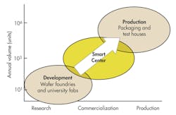
“Packaging, testing, and the manufacturing method are all highly dictated by the application for MEMS devices,” explains Matt Apanius, director of the Richard Desich Smart Commercialization Center for Microsystems at Lorain County Community College (LCCC) in Elyria, Ohio, a MEMS foundry for packaging, assembly, and test on an accelerated time-to-market basis (Fig. 2).
The LCCC Center develops manufacturable packaging integration solutions for customers developing next-generation micro-system products by leveraging leading-edge facilities and highly knowledgeable engineering teams. The State of Ohio Department of Development program, which aims to bring manufacturing facilities back to the state, many of which have gone overseas, generously funds it with the college.
This file type includes high resolution graphics and schematics.
“This is vital in applications like bio-MEMS where extremely small size MEMS pressure sensor ICs are required as in guided-wire cardiovascular catheterizations where catheters as small as 350 µm in diameter are used,” Apanius adds. The sensors are needed to determine the amount of stenosis,an abnormal narrowing in a blood vessel or other tubular organ or structure.
Microfluidic MEMS devices are being increasingly used in medical, pharmaceutical, life-sciences, and in-vitro diagnostic applications. This a growing market according to Yole Développement, which expects it to increase swiftly from $1.4 billion this year to $5.7 billion by 2018, an impressive 27% growth rate.
SF Fluidics in the U.S. is collaborating with Singapore’s A*STAR Institute of Microelectronics to develop a portable diagnostic tool to rapidly triage traumatic brain injury (TBI) victims. The microfluidic tool is a fully automated biosensor that requires only a drop of blood to detect up to three biomarkers released by the brain after an injury. TBI is one of the most common causes of death and disability in the world, resulting from blasts, falls, knocks, traffic accidents, and assaults.
Inertial Sensors Improving
Performance levels for MEMS accelerometers and gyroscopes are consistently getting better. Some MEMS sensors include the accelerometer and gyroscope in the same package. They’re seeing greater use in the automotive sector spurred on by the car safety systems now mandated by the government. These sensors provide inertial inputs to a car’s electronic stability control (ESC) system and can save a lot on packaging costs and space.
The MPU-6500 six-axis chip from Invensense combines a three-axis accelerometer and a three-axis gyroscope as well as an onboard digital motion processor in a 3- by 3- by 0.9-mm quad flat no-lead (QFN) package. It operates from 1.8 V and consumes only 6.1 mW in the full operating mode. The accelerometer features a typical offset of only ±60 mg and 250 µg/√Hz of noise, and it draws only 18 µA of current in the low-power mode. The gyroscope features a ±5°/s zero-rate-output and 0.01°/s/√Hz of noise.
Smart phones are one target for MEMS sensors like the Invensense MPU-6500. The chip also can be found in many other consumer electronics applications like tablets, gaming consoles, and navigation devices. Juniper Research expects smart phones to generate nearly $8 billion in revenue by 2018.
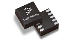
Freescale Semiconductor is aiming at the exploding smart-phone market with its MMA865xxFC three-axis accelerometer, which exemplifies a new generation of small-form-factor, power-thriftier, better noise-proof and higher-resolution devices yet is lower in cost. In a 2- by 2-mm ultra-small package, the FC Xtrinsic accelerometer consumes just 7 µA of current, has 150-µg/√Hz low noise, and boasts a sensitivity of 1 mg/LSB. It costs just 77 cents (U.S) in large-volume lots (Fig. 3).
Smart-phone designers can now avail themselves of tunable RF MEMS digital variable capacitor ICs from Cavendish Kinetics for the front end of their designs to improve the quality and connectivity of wireless coverage between their phones and towers. They’re available in chip-scale packages (CSPs).
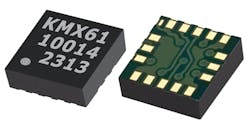
Many mobile devices can benefit from Kionix’s KMX61G six-axis MEMS accelerometer/gyroscope/magnetometer with leading proprietary sensor-fusion software that delivers highly accurate gyroscope emulation and draws a mere 550 µA of current in a 3- by 3- by 0.9-mm package. This dramatic reduction of power consumption versus conventional gyroscopes enables applications previously unreachable using traditional nine-axis solutions (Fig. 4).
“We see many applications in mobile devices that can benefit from gyroscope functionality but do not require extreme performance of a traditional gyroscope. This magnetic gyroscope can meet these needs well while offering power, cost, and size benefits that are very attractive,” says Jeremie Bouchard, director and senior principal analyst at IHS Suppli.
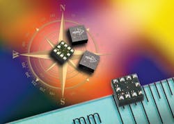
To reduce the cost and increase the number of applications for magnetic sensing, MEMSIC introduced the MMC246xMT two-axis magnetic sensor. Provided in a miniature 2.0- by 2.0- by 1.0-mm land-grid array (LGA) package, it can operate from a single 1.8-V supply and offers the industry’s best performance at the lowest power consumption for a two-axis magnetic sensor, making it ideal for portable applications (Fig. 5). It’s designed for electronic compassing, in-vehicle GPS assist, GPS wristwatches, and industrial field measurements including traffic control and parking management.
The MMC246xMT is made using MEMSIC’s proprietary anisotropic magnetic resistive (AMR) technology to achieve its high performance. Operating over the range of ±6 Gauss full scale, its full integration provides all of the necessary circuit functions to facilitate its design into systems while saving space, reducing cost, and increasing reliability over currently available solutions that require external circuit elements.
The sensor also exhibits superior performance in critical electrical design parameters including dynamic range, accuracy over temperature, and power consumption. Its low noise of 0.8-mG total RMS and resolution of 0.25 mG per least significant bit (LSB) result in a more accurate heading determination with less averaging in addition to a bias error of less than ±2 mG over the –40°C to 85°C temperature range.
The low operating current of 20 µA (in 14-bit mode) and 50 µA (in 16-bit mode) along with its less than 20 nA of current in the power-down mode also make it the most energy efficient two-axis magnetic sensor commercially available today, claims MEMSIC, extending battery life to accommodate the stringent power budgets demanded in portable applications.
Smart phones and tablets may use better displays derived from digital light processing (DLP) technology developed by Texas instruments (TI) that uses micro-mirrors. At last year’s Society for Information Display (SID) Display Week in Canada, Qualcomm showed off its Mirasol MEMS-based display technology with a 5.1-in. diameter display. Mirasol uses ambient light and MEMS to create small air gaps. As their size changes, the light color passing through the air gaps is manipulated.
The company says Mirasol displays may show up in small-screen consumer devices with displays of 1.5 in. in diameter like cell phones and watches this year. Qualcomm appears to have overcome some of the obstacles of the Mirasol technology to achieving larger-size and higher-resolution displays.
Mirasol boasts very low power dissipation, up to six times less than conventional LCDs and organic LED (OLED) displays, and very high-resolution color. The demo at the SID event showed great resolution of 2564 by 1440 pixels with a pixel density of 577 pixels/in. The Samsung Galaxy 4S smart phone has a comparative resolution of just 440 pixels/in. and a resolution of 1920 by 1080 pixels. Could this be the next display for the potential Apple iWatch?
TI also is actively looking into applications for its MEMS DLP technology beyond projection products. “Engineers have been trying to rip apart projectors to use the DLP for their new ideas, so we formed a product line around these interests,” says Gina Park, TI’s product line manager. For example, a doctor in Europe has used DLP to create a photolithography tool to protect the skin of psoriasis patients from damaging ultraviolet (UV) rays by focusing the UV treatment light only onto the infected areas.
TI sees many promising applications, such as 3D printing for making precision molds for hearing aids and jewelry as well as dental scanning to map a tooth or make a crown mold. There’s also 3D machine vision for fast and precise industrial inspection and measurement. According to TI, commercialization into these areas involves optimizing the window for UV transmission and enhancing the DLP control software.
Industrial And Building Automation
The industrial sector is ready to make wider use of MEMS devices, which offer reliability, scalability, sensitivity, and cost-effective solutions. MEMS-based sensors and actuators have experienced a slow yet steady growth in industrial automation to measure and control pressure, flow, level, temperature, vibration, acceleration, tilt, and other functions.
As the industrial arena moves toward intelligent, distributed, and wireless monitoring and control, MEMS technology will likely play an increasingly vital role. Recognizing this, Analog Devices has introduced the ADIS 16229 iSensor wireless vibration MEMS sensor node. It combines dual-axis digital MEMS acceleration sensing with advanced frequency- and time-domain signal processing.
“The primary driver of predictive maintenance is the reduction of factory system downtime, which currently relies on periodic offline performance trend analysis,” explains Bob Scannell, Analog Devices’ iSensor business development manager, MEMS/Sensors Group. “With MEMS-based vibration sensors that continuously monitor machine tools, turbines, pumps, conveyors, compressors, engines, and other equipment, factory operators receive real-time statistical performance data and process control feedback that allow them to prevent costly system shutdowns.”
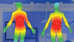
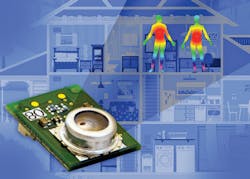
Omron recently introduced a non-contact D6T MEMS thermal sensor that can reliably detect the presence of people without needing them, aimed at creating advanced new energy appliances for the home, building automation, and factory automation applications (Fig. 6). It offers ±1.5°C accuracy and 140-mK noise immunity (measured as equivalent temperature difference).
According to Omron, the D6T is more reliable than conventional pyroelectric, infrared (IR), and passive IR (PIR) sensors used in industrial, building, and home automation applications. It uses a MEMS micro-mirror structure for efficient for IR radiation detection with a high-performance silicon lens to focus the IR rays onto thermopiles. Proprietary ASICs make the necessary computations and convert sensor signals into digital ones for output to an I2C bus.
Relative sensing and temperature are two important measurement and control parameters in industrial environments. The MVH300D series of digital relative humidity and sensing chips from MEMS Vision offers a combination of high-performance features. The company capitalizes on its expertise in MEMS and ASICs and on its revolutionary MoSiC platform to offer a range of environmental sensing products and advanced MEMS-based solutions.
There series boasts ±1.5% relative humidity accuracy (the MVH3001D), superior ruggedness, reliability, and durability, thanks to the use of silicon-carbide (SiC) technology. It also offers a rapid response time of 6 s typical, small package size of just 2.4 by 3 by 0.8 mm, and extremely low power consumption of 2 µW for each relative humidity and temperature measurement/s (at 1.8 V and 8-bit resolution). Temperature measurement accuracy is guaranteed to be within ±0.2°C to ±0.3°C.
Summary
There’s plenty of room for MEMS technology to grow, but many sensor types need time to mature and become more widespread. Roger Grace of Roger Grace Associates points out that more improvements are needed in “design for manufacturing and research and development, two efforts that are ongoing.” There’s also a need for better marketing efforts and greater venture capital funding.
This file type includes high resolution graphics and schematics.
About the Author
Roger Allan
Roger Allan is an electronics journalism veteran, and served as Electronic Design's Executive Editor for 15 of those years. He has covered just about every technology beat from semiconductors, components, packaging and power devices, to communications, test and measurement, automotive electronics, robotics, medical electronics, military electronics, robotics, and industrial electronics. His specialties include MEMS and nanoelectronics technologies. He is a contributor to the McGraw Hill Annual Encyclopedia of Science and Technology. He is also a Life Senior Member of the IEEE and holds a BSEE from New York University's School of Engineering and Science. Roger has worked for major electronics magazines besides Electronic Design, including the IEEE Spectrum, Electronics, EDN, Electronic Products, and the British New Scientist. He also has working experience in the electronics industry as a design engineer in filters, power supplies and control systems.
After his retirement from Electronic Design Magazine, He has been extensively contributing articles for Penton’s Electronic Design, Power Electronics Technology, Energy Efficiency and Technology (EE&T) and Microwaves RF Magazine, covering all of the aforementioned electronics segments as well as energy efficiency, harvesting and related technologies. He has also contributed articles to other electronics technology magazines worldwide.
He is a “jack of all trades and a master in leading-edge technologies” like MEMS, nanolectronics, autonomous vehicles, artificial intelligence, military electronics, biometrics, implantable medical devices, and energy harvesting and related technologies.
Voice Your Opinion!
To join the conversation, and become an exclusive member of Electronic Design, create an account today!

Leaders relevant to this article:
