16nm/14nm FinFETs: Enabling The New Electronics Frontier
The next frontier in the electronics industry is the FinFET, a new type of multi-gate 3D transistor that offers tremendous power and performance advantages compared to traditional, planar transistors. Intel is already using FinFET technology (called "tri-gate") at 22nm, and many foundries are now preparing 16nm or 14nm FinFET processes. While the technology has compelling advantages, it also poses some new design challenges, and its success will require extensive R&D and deep collaboration across the semiconductor design ecosystem.
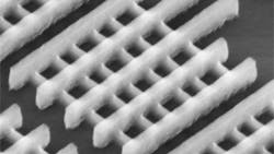
FinFETs are field effect transistors (FETs) that get their name because the transistor gate wraps around the transistor's elevated channel, or "fin." This approach provides more control over current than planar transistors can achieve, and it reduces both leakage and dynamic power. A 16nm/14nm FinFET process can potentially offer a 40-50% performance increase or a 50% power reduction compared to a 28nm process. While commercial foundries will first offer FinFETs at 16nm or 14nm, some foundry processes will keep the backside metal layers at 20nm, potentially easing the migration to FinFETs.
Will there still be a role for 20nm planar transistors? Over time, that's a good question, but here at the beginning of 2013, 20nm planar processes are going into full production and 16nm/14nm FinFET volume production is still a year or two away. There are still many unknowns around FinFET cost and yield. But as time goes on, we expect strong interest in FinFET technology, particularly for next-generation mobile consumer devices.
Like any new technology, FinFETs pose some design challenges, especially for custom/analog designers. One is sometimes called "width quantization" and it stems from the fact that FinFETs work best as regular structures placed on a grid. Standard cell designers can change the width of a planar transistor, but they cannot change the height or width of a fin, so the best way to increase drive strength is to add more fins. This must be done in discrete increments - you can't add three-quarters of a fin.
Another challenge stems from the 3D topology itself, which increases the number of resistance (R) and capacitance (C) parasitics that must be extracted and modeled. No longer can designers just model transistor length and width - the Rs and Cs inside the transistor, including local interconnect, fins, and gates, are critical for predicting the transistor's behavior. Yet another issue is layer resistance. The 20nm process added a local interconnect layer below the metal 1 layer, and its resistivity distribution is non-uniform and dependent on where the vias are placed. Further, there can be a 100X difference in resistivity between the top metal layers and the lower metal layers.
There are also challenges that have more to do with the smaller geometries at 16nm and 14nm than FinFETs themselves. One is double patterning, which is needed at 20nm and below to get features to print correctly with current lithography equipment. It requires extra masks, along with a colorized decomposition process that determines how layout features will be implemented by different masks. Layout-dependent effects (LDE) occur because layout features that are placed near to a cell or device will impact its timing and power. Electromigration becomes more of a concern as geometries shrink.
As noted, the above-mentioned issues primarily impact custom/analog designers. If a digital designer has automated, FinFET-aware tools and characterized libraries, the main difference he or she will notice is the better power and performance characteristics of the cells. But digital designers may also notice new and complex design rules, double-patterning colorization requirements, and more restrictions on access to cells and pin locations. Finally, some SoC designers will be asked to design and verify a chip that has hundreds of millions of gates. Designers will need to work at higher levels of abstraction and heavily reuse silicon IP.
The EDA industry is spending a great deal of money on R&D to ease advanced node design challenges - in fact, we expect that that total EDA industry expense may reach $1.2 billion to $1.6 billion for 20nm, 16nm, and 14nm processes combined. From a FinFET perspective, for example, extraction tools must be enhanced in order to handle the Rs and Cs necessary to predict transistor performance. Those Rs and Cs can't wait for post-layout analysis - they need to be brought into the design cycle earlier, calling for a change in methodology in which circuit designers and layout designers work more closely together.
Every physical design tool must be able to handle several hundred new design rules that 16nm/14nm FinFET processes will bring. This includes placement, routing, optimization, extraction, and physical verification. The cell library should be co-optimized with these tools, a task made easier with an integrated advanced-node solution that encompasses both custom/analog and digital design.
EDA vendors are one part of a vertical collaboration that also includes foundries and IP providers. Feedback from EDA and IP developers can influence process development, which in turn sets new requirements for tools and IP. In 2012, for example, a three-way collaboration between Cadence, ARM and IBM produced one of the first 14nm FinFET test chips.
Will 16nm/14nm FinFETs remain a niche technology, or enter the IC design mainstream? History proves that when new innovations are available, people figure out how to use them to create new and often unexpected value. FinFETs stand poised to enable the next big leap for computer, communications, and consumer devices of all types. That's why Cadence believes that FinFETs represent a new frontier for the electronics industry, and why we're committed to enabling that technology for the industry at large.
About the Author
Chi-Ping Hsu
Senior Vice President, Research and Development, Silicon Realization Group
Chi-Ping Hsu is senior vice president of research and development for the Silicon Realization Group. In this role which is now aligned with the industry EDA360 vision, he is responsible for the core business that encompasses silicon design, verification and implementation, and includes signoff/DFM, package and board. His role is critical to efficiency, quality and product competitiveness.
Hsu previously served as chief strategist of products and technologies and corporate vice president and general manager of both synthesis solutions and digital IC implementation. During his tenure, Cadence® grew its presence in the synthesis segment tenfold, and the company made significant quality and technology advancements in digital IC implementation.
In addition, Hsu was the visionary behind the Cadence Low Power Solution and the primary driver of Power Forward, the industry's leading initiative organization focused on enabling the development of power-efficient ICs and electronic systems. Prior to joining Cadence in 2003, Hsu served as president and chief operating officer of Get2Chip Inc. and before that held executive management positions at Avant! Corporation, where he was responsible for corporate and technology strategy, product development and marketing.
Hsu holds a Ph.D. degree in EECS from the University of California, Berkeley, and a BSEE degree from National Taiwan University.
Comment About the Article
To join the conversation, and become an exclusive member of Electronic Design, create an account today!

Leaders relevant to this article: