FinFETs Herald A Seismic Shift In Semiconductor Technology
Since the inception of the integrated-circuit (IC) industry, design metrics such as performance, power, area, cost, and time-to-market have remained the same. In fact, Moore’s law is all about optimizing those parameters to produce the smallest possible transistor size with each new technology generation.
However, as process technologies gradually shrank toward 20 nm, it became impossible to achieve a similar scaling of certain device parameters. This was particularly true for power-supply voltage, which is the dominant factor in determining dynamic power. In addition, optimizing for one variable (e.g., performance) automatically translated to unwanted compromises in other areas (e.g., static power).
Faced with the new emerging metric of performance per unit power (Koomey’s law), engineers are looking to optimize their designs via an alternative technology: the FinFET. Compared to planar technology, FinFETs offer much better performance at the same power budget, or equal performance at a much lower power budget.
In terms of Moore’s law, it’s reasonable to infer that FinFETs represent the most radical shift in semiconductor technology in over 40 years. When Gordon Moore came up with his “law” back in 1965, he perceived a design of about 50 components. Today’s chips consist of billions of transistors, and design teams strive for “better, sooner, cheaper” products with every new process node. However, ever-finer feature sizes potentially introduce the perils of high leakage current due to short-channel effects and varying dopant levels, which ultimately threaten to derail the industry’s progress to smaller geometries.
The FinFET transistor structure promises to rejuvenate the chip industry. It will do so by reducing the short-channel effects that limit device scalability faced by current planar transistor structures.
FinFET: A Technology Primer
The FinFET’s technology roots trace back to the 1990s, when the U.S. Defense Advanced Research Projects Agency (DARPA) looked to fund research into possible successors to the planar transistor. A University of California at Berkeley team, led by Dr. Chenming Hu, proposed a new structure for the transistor that would reduce leakage current.
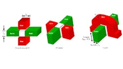
The Berkeley team suggested that a thin-body MOSFET structure would control short-channel effects and suppress leakage by keeping the gate capacitance closer to the whole of the channel. The researchers proposed two possible structures (Fig. 1).
1. FinFET transistors originated from thin-body MOSFETs, a concept initially explored by a research team from UC Berkeley.
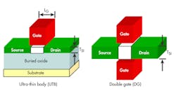
Rotating the double-gate (DG) structure, which has the potential to provide the lowest gate leakage current, enables easier manufacturing using standard lithography techniques (Fig. 2). The gate electrodes become self-aligned. Overall, the layout is similar to that of a planar FET.
2. The double-gate (DG) structure used in planar FET, when rotated, helps form the FinFET.
Modern FinFETs are 3D structures that rise above the planar substrate, giving them more volume than a planar gate for the same planar area. Given the excellent control of the conducting channel by the gate, which “wraps” around the channel, very little current is allowed to leak through the body when the device is in the Off state. Consequently, lower threshold voltages can be used, resulting in optimal switching speeds and power.
Other research teams have shown that FinFETs are scalable as long as it’s possible to scale the thickness of the channel. For example, the Korea Advanced Institute of Science and Technology (KAIST) has demonstrated a 3-nm FinFET in its lab.
The FinFET Promise
Leading foundries forecast that the processing of 3D devices will cost 2% to 5% more than that of planar wafer fabrication. Estimates show that FinFETs will be up to 37% faster while using less than half the dynamic power, or cut static leakage current by as much as 90%.
FinFETs also promise to alleviate problematic performance-versus-power tradeoffs. Designers can accelerate the transistors using the same amount of power, compared to the planar equivalent, or run them at the same performance using less power. Thus, design teams can balance throughput, performance, and power to match the needs of each application.
Design Challenge: Minimizing Impact
Designers these days tend to care less about packing as many transistors as possible on a die (Moore’s law) and more about delivering the best performance per watt for the application. Interestingly, Jonathan Koomey has shown that the energy efficiency of computers has doubled nearly every 18 months since the first computers were built in the 1950s.
Koomey’s law expands on Moore’s law, particularly when considering the diminishing relevancy of quoting channel lengths. Given the abundance of transistors per unit area in advanced nodes, designers use multiprocessors at lower voltage to achieve the same throughput of a fewer number of processors at a higher voltage. This would sacrifice some additional area for the sake of saving power at the same throughput level.
The foundries want to make the transition to FinFET processes as transparent and smooth as possible for the design community. To do that, the EDA and IP industries must work behind the scenes to ensure that the tools can understand and model all of the complexities. Design teams want to take advantage of the power, performance, and area benefits offered by FinFETs, while still getting to market quickly and painlessly through a familiar process of creating the RTL and taking it through a backend implementation process.
IP Challenges: Not Just Another Transistor
Developers can take a familiar design flow and work with FinFET technology very much like they did with previous bulk CMOS designs. However, the quality of results will depend greatly on the quality of the IP.
Developing optimized memory and standard cells (physical IP) for FinFETs requires expertise and experience. An experienced design team will be able to exploit FinFET features to create the best physical IP and not leave any power savings or performance on the table. To continue on the path of Moore’s law (and Koomey’s law), designers must be able to leverage the target technology for maximum benefit. Invariably, that means focusing on the details.
A key challenge with FinFET technology is the discrete size of the fin. Transistor width (W), one of the main variables for tweaking transistor sizes, is no longer a continuum. Discrete fin sizing brings a new variable in design, without any easy workaround. Furthermore, additional design levers typically used by IP designers, such as varying the channel length or body biasing, are either much more restrictive or offer little benefit due to the intrinsic characteristics of FinFET technology.
Another challenge concerns the model’s complexity. Because the FinFET is a 3D structure, it has lots of subdivided resistance and capacitance compared with a planar structure. This 3D structure requires a more complex model and more data manipulation than planar transistors. Such complexity has implications for the whole backend flow, including extraction, layout, design rule checks (DRCs), and layout versus schematic (LVS), for the engineers managing the design.
Experience Counts
When it comes to IP design, experience is needed to squeeze the most out of FinFET technology. On this front, Synopsys spent several years researching the characteristics of FinFET technology and applying them to create new standard cell architectures and memory compilers. For instance, the company exploited the inherently low operating voltages of FinFETs to enable the design of memories with low retention voltages.
Another fundamental issue that determines a transistor’s performance is its stress profile—the mechanical stress that’s deliberately introduced into the device to enhance its performance. Because of its vertical fin, the FinFET has a significantly different stress profile than a planar transistor. Synopsys has been collaborating with industry partners from an early stage to apply its Technology Computer-Aided Design (TCAD) tools to the task of accurately modeling FinFET stress profiles.
The company works closely with the major foundries to capture all intricacies of FinFET technology and create models that are usable within the entire design flow from concept to implementation, including Spice modeling, extraction, and physical IP design. The foundry’s intent is to ensure the transition to FinFET is as transparent as possible so users can seamlessly scale designs to increasingly smaller geometry processes.
Maximum benefits with this technology will require implementation tools to minimize power consumption and maximize utilization and clock speed. FinFETs require some specific enhancements in:
• TCAD tools
• Mask synthesis
• Transistor models
• Spice simulation tools
• RC extraction tools
• Physical-verification tools
TCAD Tools
Wafer-processing technologies are being developed to harness the full potential of 3D FETs. They will controllably dope the fin sidewalls and stress the fins to help boost device performance. To support these efforts, foundries are using TCAD tools during development to guide and optimize the semiconductor fabrication process.
The need for 3D TCAD simulation is no more evident than in the process optimization of SRAM cells, where stress and doping proximity effects require all SRAM transistors to be simulated in a single structure. Recent advances in 3D structure generation, mesh generation, and parallel algorithms make it possible.
The small geometries targeted for FinFETs cause concern regarding the impact of process variability on device and circuit performance. While these effects were negligible on higher geometry processes, they’re now becoming first order effects. Created by random dopant fluctuations, line-edge roughness, layout induced stress, and other process variations, they manifest themselves as variations in device performance, particularly with threshold voltage shifts and local currents that influence timing and power. TCAD tools simulate these effects and, ultimately, help build the device models used by EDA tools.
Synopsys has deployed Sentaurus TCAD in FinFET research and development since 2005 at foundries, integrated device manufacturers (IDMs), and research universities, and it has made highly complex and sophisticated refinements to these tools as a result of these collaborations. Refinements include changes to the company’s plasma-doping model; fin dimensional optimization to achieve device performance targets; and modeling of the random process variations to improve device performance. For example, Sentaurus can perform 3D simulation for p-channel FinFETs (Fig. 3).
3. Stress fields in p-channel FinFETs were simulated with Synopsys’ Sentaurus TCAD tool.
Mask Synthesis
Mask synthesis, a key component in advanced manufacturing, post-processes the resultant layouts produced by EDA tools and helps compensate for limitations and effects in manufacturing lithography processes. The advanced geometries targeted for FinFET are expected to require self-aligned double patterning (SADP) in deposition manufacturing steps to create the fins rather than lithographically defining the fins. Because the fins are tall and thin, traditional lithography/OPC methods would result in line-edge roughness problems.
Synopsys developed Proteus to address these issues. It performs full-chip proximity correction, builds models for correction, and analyzes proximity effects on corrected and uncorrected IC layout patterns. The company is closely engaged with foundries on refining and deploying the Proteus SADP solution.
Transistor Models
FinFETs introduce much higher complexities for resistance and parasitic capacitance. Additional information is needed in the model for source/drain resistance extensions, contact resistances fringing effects, and the wider number of coupling capacitances introduced by the three-dimensional structures. The new behaviors are captured in the latest standardized models used by Spice simulators. For example, Spice simulators exploit the Berkeley Short-channel IGFET Model for Common Multi-Gate (BSIM-CMG) compact model to ensure accurate simulation of designs using FinFETs.
Spice Simulation Tools
FinFET foundries have used Synopsys’ Spice and FastSPICE simulators to validate correct and accurate functionality with the new BSIM-CMG models. These tools form the cornerstone for transistor-level library and circuit design. Beyond support for BSIM-CMG models, Synopsys also developed HSPICE and FineSim SPICE for full Spice accuracy, as well as CustomSim and FineSim Pro for FastSPICE use.
Resistance/Capacitance (RC) Extraction Tools
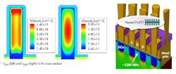
The 3D nature of FinFETs and the multiple fins making up the transistors introduce many new parasitic resistance and capacitances that must be considered, modeled, and extracted from FinFET-based designs (Fig. 4). Interconnect modeling of semiconductors has been standardized in the open-source Interconnect Technology Format (ITF). It’s recently been extended to add the FinFET requirements.
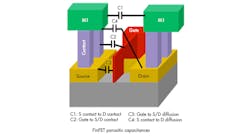
4. The FinFET’s makeup introduces new parasitics that must be modeled and extracted.
To this end, Synopsys enhanced its StarRC tool to support the new ITF models in the extraction of FinFET-based designs. StarRC is certified by leading FinFET foundries and has become the industry standard for signoff extraction.
Physical-Verification Tools
FinFET technology also will have an impact on physical verification. The new runsets employed by physical-verification tools are used to verify LVS correctness and DRCs. FinFETs require LVS enhancements to support recognition of these new devices in the layout and to enable parameter extraction and identification of proximity effects. Other LVS enhancements include new source-drain resistance calculations. Some of the latest design rules to be introduced include fin-to-fin spacing and fin widths.
To support LVS and DRC for FinFETs, Synopsys enhanced its IC Validator physical-verification tool. It’s currently being used in the development of FinFET- based designs and IP.
The Synopsys TCAD and Galaxy Implementation Platform of tools, including IC Compiler, Galaxy Custom Designer, and PrimeTime, have already been used to tapeout 3D FET production designs and test chips. Now they’re ready to handle the next wave of FinFET technology adopters. The entire design flow from concept to implementation includes Spice modeling, extraction, and physical IP design (Fig. 5).
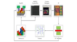
5. Spice modeling, extraction, and physical IP design are all involved in Synopsys’ FinFET design flow.
Summary
Historically, design teams have transitioned their IP from older planar technologies to the latest process nodes by using in-house design capabilities and IP reuse. FinFET technology has created new challenges because current tools and techniques may not enable these teams to design their IP optimally for FinFET processes, delaying time to market. FinFETs require a new generation of design experience, expertise, and tools to get the most from the technology. By leveraging Synopsys’ experience with FinFETs, design teams may be able to mitigate the risk in developing FinFET-based IP processes.
Jamil Kawa, group director in the Solutions Group at Synopsys, holds an MSEE from the University of Michigan, Ann Arbor, and an MBA from Santa Clara University, Calif. He can be reached [email protected].
Andy Biddle, product marketing manager in the Implementation Group at Synopsys, holds a bachelor of science degree in electrical and electronic engineering from London South Bank University, United Kingdom. He can be reached at [email protected].
About the Author
Comment About the Article
To join the conversation, and become an exclusive member of Electronic Design, create an account today!

Leaders relevant to this article: