Make The Leap From Test Chips To Production Designs At 20 nm

2012 was the year of test chips for the 20-nm technology node. Most leading fabless semiconductor companies spent 2012 preparing for their first production designs that will be taping out in 2013. As we start the transition from test chip evaluation to real production, it is perhaps a good time to reflect back on what we have learned about the IC design process for 20 nm.
Does DP Coloring Make Debug Easier?
Custom design has always been challenging, but never so much as at 20 nm, where layouts must now comply with double patterning (DP). Some custom design tool suppliers advocate using their tools to decompose the layout into two masks—a process called “coloring,” since the mask assignments of layout polygons is typically represented by displaying the polygons in two different colors. They claim that showing the mask coloring makes finding and fixing DP rule violations (i.e., DP debugging) easier. But that isn’t usually the case. Why?
Unlike DRC spacing errors, which usually have one correct solution that is fairly obvious once the rule violation has been described, there can be many correct ways to color a set of polygons (Fig. 1). However, when a DP rule violation occurs, this flexibility can make fixing DP violations much trickier.
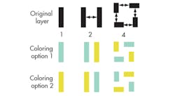
Figure 1. For most designs, there can be many equally correct decomposition solutions.
For example, one of the most common types of violations is the “odd-cycle” error, where an odd number of closely spaced adjacent polygons (e.g., 3, 5, 7) must be decomposed. You can separate two of the polygons by putting them on different masks (coloring them differently). But with double patterning, you only have two masks, and therefore only two colors. Each possible “pair” of polygons in this trio must be different colors, but that is impossible. So what about the third polygon—what color should it be?
When a signoff DRC/DP tool finds an odd-cycle DP error, no simple coloring solution can resolve the conflict. The designer must make spacing changes to the layout, or add or remove polygons, and the possible solutions can be numerous (Fig. 2). In this case, showing only some of the different coloring options doesn’t make debug easy. It can be confusing at best, or even misleading to the designer.

Figure 2. An odd-cycle error in a DP layout can have many different apparent fixes.
The problem is that some of the possible changes will, in fact, create new odd-cycle errors or other DP violations, which may be more complex and difficult to fix than the original error. How does the designer avoid falling into this black hole?
What is useful to designers in this scenario is a type of visual feedback that shows all the polygons involved in the odd-cycle error as part of an “error ring.” The error ring visualization helps designers avoid simplistic corrections that might actually create a cascade of additional DP errors. Taking this a step farther, a predictive DP error debugging process can forecast how and where the odd-cycle DP error might expand if the correction is not made in the right place.
Figure 3 illustrates both the DP error rings (in red) and predictive warning paths (in yellow). In this case, the warning rings indicate that fixes will not be successful if they are applied to the edges touching the error rings. Instead, the designer should make fixes to the bottom-facing edges of the affected polygons, where the rings are not touching the polygons.
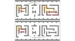
Figure 3. Error rings are useful debugging aids that point designers to the right locations to correct a DP error without creating new violations. (Warning paths are patent pending by Mentor Graphics.)
Know And Control Your Design’s Coloring
The decomposition of layers into two masks at 20 nm introduces a new source of design variability, because the two masks require two separate exposures, and the best overlay accuracy of advanced scanners is on the order of 4 to 8 nm. Such an overlay error will impact parasitics, which may be important for critical nets. Because of this effect, some customers are interested in explicitly understanding and controlling the coloring of critical areas/nets in their designs.
Regardless of the EDA supplier, DP decomposition and checking tools use virtual graphing techniques to assign colors and avoid cycle violations. Even if you use the same DP decomposition tool as your foundry’s OPC organization, any subtle design or configuration changes will alter the graph and subsequent design coloring assignments from run-to-run. Examples of such variations include:
- Adding or modifying layout data (moving/adding polygons, placing polygons in parent cells, adding frame/scribe lines, adding fill, etc.)
- EDA tool release-to-release changes (database construction, enhancements, optimizations, etc.)
- Execution mode changes (runtime options)
- Distributed computing environment changes (# CPU cores, hardware configurations, etc.)
Changes in the coloring create subtle differences in the masks, which can affect the value of parasitics (and therefore the timing of critical paths). If controlling the coloring of certain portions of a design is important, the best way is to use a DRC/DP tool that generates DP coloring assignments simultaneously with DRC and DP checking. That way, designers have an error-free final color assignment that requires no additional changes.
Designers can “anchor” their design to specified colors that have passed physical verification signoff. The reference sign-off DRC/DP tool used by the industry can generate coloring simultaneously with the DRC and DP checking. These colors can be output and used to anchor your design, and the major foundries have committed to honor these anchored designs from their customers. Only through this approach can you guarantee that the design is colored exactly as you intended.
New Design Methodology Concerns
To ensure the best design performance, most IC companies have had proprietary design methodology guidelines and/or DRC checks for their designers for years. With 20 nm, a new chapter must be added that considers the impact of DP coloring during IP development. In addition to all the DP single mask spacing requirements discussed above, foundries require the two DP mask layers to be reasonably density-balanced to mitigate lithographic intensity and local etch bias issues during manufacturing. The wrong design methodology color anchoring choices can make it hard to hit the density balancing checks (if any) from your foundry.
Consider the example in Figure 4, where design choices within the cell can have higher-level design and density implications. The layout on the left drives both power rails to be the same color. In doing so, this simple design methodology choice dramatically skews the overall mask A/B density balancing.
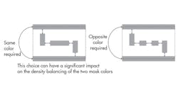
Figure 4. With double patterning, simple design choices can have significant upstream effects.
There are myriad other examples of coloring issues that must be carefully considered and added to a design team’s design methodology checks. Your takeaway—carefully consider where and how your design team chooses to anchor portions of your IP.
The Next Steps
Over the last year, as we have worked with companies creating their first 20-nm test chips, there have been some bumps in the road. Every node has its growing pains, and 20 nm is just bringing some new and interesting ones. Fortunately, we have also discovered some relatively straightforward solutions along the way. To summarize some of the 20-nm lessons:
- Don’t rely on viewing assigned coloring alone to debug DP errors. Look for tools that provide coloring debug aids that can predict the best ways to fix a violation.
- If understanding and controlling the coloring of critical areas of your design is important, use the golden sign-off DRC/DP tool used by the industry to generate coloring simultaneously with DRC and DP checking to anchor the color of your critical design areas. Only with this approach can you guarantee that a design is colored exactly as you intended. Any other approach will add additional steps to your verification/tape-out process, and the final mask set used to manufacture your design may be different than what your designer intended.
20-nm design brings new design methodology checks with DP coloring. So in light of DP coloring requirements, carefully consider your custom design methodologies and checks, as choices at the cell level can have unforeseen impacts at the chip level. Next year will be exciting as the industry moves forward into 20-nm production and takes advantage of the scaling and performance benefits the new node can offer.
About the Author
Michael White
Michael White is Director of Product Marketing for Mentor Graphics’ Calibre Physical Verification products. Before joining Mentor Graphics, he held various product marketing, strategic marketing and program management roles for Applied Materials, Etec Systems and the Lockheed Skunk Works. Michael received a BS in System Engineering from Harvey Mudd College. He also holds a MBA/BS in engineering management from the University of Southern California.
Comment About the Article
To join the conversation, and become an exclusive member of Electronic Design, create an account today!

Leaders relevant to this article: