Q&A: MACOM’s Doug Carlson Discusses GaN’s Market Potential and Trajectory
In terms of mainstream adoption, gallium nitride (GaN) has reached a crossroads of technology innovation and supply-chain transformations. GaN offers significant advantages when it comes to semiconductors. It’s been used in RF and LED applications, and can be effective in solar applications, too.
One company that’s working with GaN technology is MACOM. I spoke with Doug Carlson, Vice President of Strategy, about where GaN is headed and what is changing in the industry.
Wong: Do you consider gallium nitride a “proven” technology at this point, or are the industry’s expectations for GaN’s performance still in flux?
This file type includes high resolution graphics and schematics when applicable.
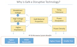
Carlson: The performance advantages achievable with GaN technology are well known within the RF and microwave industry today. GaN delivers as much as 8X the raw power density of incumbent GaAs and LDMOS technologies at high efficiency, with the ability to scale the device technology to high frequency. GaN technology has also allowed device designers to achieve broad bandwidths while maintaining high efficiency (Fig. 1). These are proven benefits.
Many of the early reliability challenges of GaN have been solved and GaN today demonstrates, via RF life test, a mean time to failure (MTTF) of greater than106 hours at a junction temperature above 200°C. Though GaN has realized many significant advances over incumbent technologies, GaN has not realized its full potential. Over the coming years, we expect advances in total power per device, penetration of GaN into additional RF functions, and increased functional integration.
Wong: How would you characterize GaN’s early market trajectory?
Carlson: Historically, GaN technology development has been primarily driven by government funding and R&D. GaN on silicon carbide (SiC) is being successfully applied in the military domain today, in applications such as broadband electronic warfare jammers and radar systems, while GaN on silicon (Si) has been successfully deployed in military communications. GaN’s usage continues to expand in the military market. These initial successes have opened the door for its penetration into commercial markets, including CATV, cellular infrastructure, and other applications. In fact, we are seeing the initial penetration of GaN into these markets.
Today, we are only at the very beginning of GaN market penetration and adoption. GaN revenue for 2013 was $188.6M according to ABI Research, suggesting that the technology has penetrated less than 1% of the approximate $9.5B overall analog semiconductor market. Given the extensive hype around GaN, this narrow market penetration may come as a surprise to many, especially when one measures GaN’s potential impact beyond the RF and microwave market. It’s been said that there isn’t a single analog function that won’t be made better with GaN. Indeed, when GaN’s cost structure comes into alignment with incumbent technologies, its disruptive effect on the analog domain will be massive.
Wong: What applications do you expect to be the biggest market growth drivers for GaN technology in the near term?
Carlson: In the RF field, in the near term, GaN will see the highest growth in cellular infrastructure applications. GaN’s bandwidth, power, and efficiency advantages provide compelling drivers for adoption in macro base stations and small cells. It will further penetrate cellular infrastructure, providing solutions for point-to-point communications. While military use of GaN will remain solid and in fact grow, the commercial market will continue on its present trend and be the main driver today and in the future.
GaN will have a profound impact on the microelectronics industry beyond RF applications. GaN, particularly GaN on Si, is poised to revolutionize the power-conversion market, which seeks an improved semiconductor platform for high-voltage power management. Many of the fundamental properties that make GaN a compelling solution for RF also make it the ideal solution for power conversion. This market may be as much as 10X larger than the RF and microwave market serviced by MACOM.
Wong: How do you answer skeptics who say that GaN is too expensive to support mainstream commercial applications?
Carlson: GaN, at its current cost structure, has begun to penetrate commercial applications. Its use is primarily driven by performance advantage. Further penetration into commercial markets will place significant demands on the manufacturing infrastructure for GaN—from device fabrication to packaging. The entire supply chain will have to adjust to increased market demand.
GaN-on-Si device technology coupled with high-performance plastic packaging solutions is ideally suited to address the challenges of high-volume commercial markets. Certainly GaN-on-SiC technology will continue to support less price-sensitive applications. The supply chains for GaN are defined along these two separate paths, and not surprisingly, these supply chains look very different. The cost-effectiveness of GaN ties directly to the process efficiencies and ultimate scalabilities of these supply chains.
Wong: How would you characterize and compare the respective process efficiencies and supply chains for these two flavors of GaN, and how do these factors impact cost?
Carlson: GaN on SiC will remain the purview of low-volume, niche applications due to the inherent cost structure of the substrate material. Fundamentally, at a physics level, SiC boules grow significantly slower than silicon. The main cost drivers for producing substrates—notably capital depreciation and energy consumption during growth—scales proportionally to production time. Therefore, GaN on SiC will remain perpetually higher cost, and thus prohibitive, for mainstream commercial use. The high attendant costs of producing SiC ensure that this market will be serviced by a select group of high-mix, low-volume compound semiconductor fabs.
By comparison, GaN on Si leverages the supply chain and cost structure of the broad silicon semiconductor industry. This allows GaN, as a new technology, to exploit enormous industrial manufacturing scale, both in terms of wafer diameter and sheer fabrication volume, while also benefitting from decades of optimized process control. These factors will drive the GaN-on-Si cost structure, in the near term, to be comparable to silicon solutions.
And whereas carbide is a relatively new material with a correspondingly short history of use in industrial-scale applications, silicon has benefited from more than 60 years of industrialization and development. It’s arguably the most technically engineered material on the face of the earth, so the supply chain for GaN on Si has a host of natural cost efficiencies aligned in its favor.
Wong: What will the GaN market landscape look like when it reaches full maturity?
Carlson: We expect that the GaN-on-Si cost structure in mainstream silicon fabs will be reduced significantly from today’s GaN-on-SiC structure. Scaling GaN from small-diameter GaN development fabs to 200-mm silicon fabs will achieve orders of magnitude reductions in cost.
Providing a viable roadmap for cost-effective manufacturing removes one of the last remaining barriers to mainstream GaN adoption. GaN’s cost structure will soon intersect and drop below that of GaAs for cell phones. Once cost parity is achieved, better performing technologies always displace incumbents in the highest-performance applications.
To fully realize the commercial promise of GaN, there must also be surety of supply to promote stability and resiliency—to say nothing of economic efficiency—across the GaN supply chain. Exact dual-source support is a key requirement for high-volume, risk-adverse applications.
Wong: How big a factor is GaN component packaging technology with regard to mainstream GaN adoption?
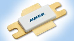
Carlson: GaN packaging options are an essential part of the equation, with implications for product performance and cost, as well as manufacturing efficiency. Recently, MACOM has focused on the introduction of high-performance, surface-mount plastic packaging for high-power GaN devices (Fig. 2). Plastic-packaged high-power GaN enables designers to adopt conventional surface-mount manufacturing approaches and their associated manufacturing efficiencies. In this way, the adoption of GaN in plastic further drives a roadmap for supply-chain cost reduction.
Wong: When should a system designer employ a GaN-on-ceramic RF device versus a GaN-on-plastic RF device?
Carlson: GaN on ceramic remains the packaging option of choice for devices that must be hermetically sealed to ensure reliable operation in environmentally challenging conditions. Ceramic-packaged GaN devices also can manage much greater power-dissipation levels than plastic-packaged alternatives available today.
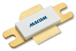
When measuring the value/useful applicability of ceramic- versus plastic-packaged GaN RF transistors, the target lifecycle for the end system is often the deciding factor. For example, military radar system designers have higher expectations for environmental ruggedness and system lifetime than designers of many consumer products. Ceramic-based GaN devices are ideally suited for systems expected to deliver extremely high reliability for long periods of time with minimal maintenance, and are often less sensitive to cost pressures than commercial-caliber systems (Fig. 3).
Wong: Are there any other hurdles to leap before GaN reaches the mass market?
Carlson: Several critical requirements must be met in order to propel GaN to mainstream market adoption, some driven by cost, and others pertaining to how we as vendors approach customers/system designers with this nascent technology. Among the practical considerations to be mindful of here is that any new technology must solve a technical problem that can’t be achieved with current technologies. In this sense, new technologies like GaN don’t replace older technologies, but rather augment capabilities and expand performance to allow the next wave of innovation. System designers and GaN vendors alike need to understand where GaN fits in the toolbox.
This file type includes high resolution graphics and schematics when applicable.
Another important baseline consideration is applications support. System designers, in general, aren’t experts in semiconductor technologies and capabilities, nor are they expected to be such. This means that vendors need to come to the table with more than just product specs; they should have the appropriate system and application-level knowledge needed to help the designer build a better product that fully captures the advantages of GaN. These challenges can be readily overcome with the right combination of designer and vendor savvy.
About the Author
Doug Carlson
Vice President of Strategy
Dr. Douglas J. Carlson received his ScB in electronic material from Brown University in 1983 and his ScD in Electronic Materials from the Massachusetts Institute of Technology in 1989. Dr. Carlson subsequently served on the research staffs of MIT and Bell Laboratory, Murray Hill, NJ. In 1990, Dr. Carlson joined MACOM in its Advanced Semiconductor Division, and is currently the company’s vice president of strategy.
William G. Wong
Senior Content Director - Electronic Design and Microwaves & RF
I am Editor of Electronic Design focusing on embedded, software, and systems. As Senior Content Director, I also manage Microwaves & RF and I work with a great team of editors to provide engineers, programmers, developers and technical managers with interesting and useful articles and videos on a regular basis. Check out our free newsletters to see the latest content.
You can send press releases for new products for possible coverage on the website. I am also interested in receiving contributed articles for publishing on our website. Use our template and send to me along with a signed release form.
Check out my blog, AltEmbedded on Electronic Design, as well as his latest articles on this site that are listed below.
You can visit my social media via these links:
- AltEmbedded on Electronic Design
- Bill Wong on Facebook
- @AltEmbedded on Twitter
- Bill Wong on LinkedIn
I earned a Bachelor of Electrical Engineering at the Georgia Institute of Technology and a Masters in Computer Science from Rutgers University. I still do a bit of programming using everything from C and C++ to Rust and Ada/SPARK. I do a bit of PHP programming for Drupal websites. I have posted a few Drupal modules.
I still get a hand on software and electronic hardware. Some of this can be found on our Kit Close-Up video series. You can also see me on many of our TechXchange Talk videos. I am interested in a range of projects from robotics to artificial intelligence.
Voice Your Opinion!
To join the conversation, and become an exclusive member of Electronic Design, create an account today!

Leaders relevant to this article:


