Clock redundancy is required for many of today’s data-communication, networking, and computer systems. Any interruption due to component or board-level failure, or even simply regular system maintenance, should not interrupt the system operation. Thus, the system clock that provides the timing for the entire circuit operation must not be interrupted under any of these abnormal circumstances. In addition, an ideal clock generator with redundancy has to provide smooth clock switching from the primary clock source to a secondary clock source or crystal upon detection of an erroneous or missing clock.
This file type includes high resolution graphics and schematics when applicable.
Common redundant clock schemes include:
• Dynamic clock switching: With this approach, the system automatically switches to a secondary clock source upon detection of a missing or erroneous primary clock source. A VCO-based PLL is required for this architecture. Dynamic clock switching requires a missing or erroneous reference-clock detector, and a circuit that can make a glitch-free and smooth transition to a secondary source.
• DCXO-based clock switching: With this approach, a digitally controlled crystal oscillator (DCXO) provides a clock source during its presence or absence of the primary reference clock source. When the reference clock is present, the DCXO is continually PLL-locked to the reference clock. During absence of the reference clock, the DCXO acts as the clock by maintaining the reference clock’s last phase and frequency state.
Dynamic Clock Switching vs. DCXO-Based Clock Switching
PLL-based dynamic clock switching provides a viable approach for the clock switching operation—if it creates smooth switching between clocks. During clock switch over, a “phase correction per cycle” (PCC) fills in (or smoothes out) the phase difference between the primary and secondary reference clocks. A large phase error between the primary and secondary clock sources could occur, producing a large phase bump in the output clock if the time to switch over isn’t long enough.
A PLL-based device should be able to minimize the phase bump by keeping the PCCs to a small value by prolonging the switch-over time. This PCC value must be small enough so that it doesn’t adversely affect the downstream PLL or setup and hold time for the synchronous system during the switch-over period.
The DCXO-based clock switching scheme uses a pullable crystal to phase-lock to the reference clock. Continuous and glitch-free operation is achieved by using a DCXO that maintains the last frequency and phase information of the reference clock in the event of primary clock failure. When the reference clock is restored, the DCXO automatically re-synchronizes this clock. DCXO-based clock switching may have certain advantages over dynamic clock switching, but it also has disadvantages:
• It requires an external pullable crystal, which are usually large in size and thus need more printed-circuit-board area.
• Limited pull range of the crystal limits the frequency lock range. As a result, maximum frequency change is approximately ±200 ppm for a normal DCXO-based device.
• The DCXO PLL’s responsiveness puts the reference switch-over time into hundreds of milliseconds.
• A low-frequency phase bump occurs due to a discrete change in frequency by switching the capacitor arrays. There are a limited number of capacitor arrays (only 10 in a typical design) to cover the entire parts-per-million (ppm) variation of the reference clock. This excessive phase noise (or phase bump) at the DCXO output can make the designer reluctant to use this device in high-performance applications.
• Due to the device’s architectural nature, the output clock carries the DCXO’s undesirable phase-noise (or phase bump) characteristics when a good reference is present, while providing a clean crystal output frequency when a reference is temporarily lost. The latter occurs because the DCXO maintains the reference clock’s last phase and frequency state without any updates and, thus, no phase bumps.
• Excessive tracking error emerges due to the DCXO-based device’s low PLL bandwidth (approximately 2 kHz).
• It can’t be used as a spread-aware device due to low PLL bandwidth.
Still, the low bandwidth of the DCXO-based architecture does offer certain advantages, especially during reference clock switching. During the time when the primary reference is lost and the device switches to a secondary reference or crystal, a longer switch time makes the PCC very small. This can result in a smooth clock switch.
An ideal smooth clock-switching device would be a PLL-based dynamic clock switch with low PCC. It may require a PLL that can lower its bandwidth from a nominal value of 1 MHz to 5-10 kHz during clock switching. With this variable PLL bandwidth architecture, it’s possible to achieve smooth clock switching.
Dynamic Switch Between Reference Clock and Crystal
PLL-based dynamic clock switching is possible not only between reference clocks, but also between the reference clock and crystal inputs. Upon detection of an erroneous or missing reference clock, the VCO can switch over to the crystal input. As long as this switch over is smooth, it will be functionally equivalent to a fail-safe device—without any of the disadvantages of the DCXO-based device (especially in regards to bullet point number 5 above). In this case, no pullable crystal is needed, and it won’t have the phase bump.
PCC for Smooth Switching
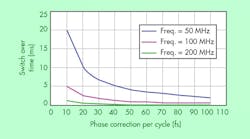
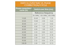
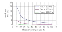
The table shows calculated switch-over times for different phase corrections per cycle at reference frequencies of 50, 100 and 200 MHz. Here, two reference clocks of the same frequency, but 180° out of phase, is assumed to be switched over. The PCC versus switch-over time curve changes at different reference frequencies (see the figure).
As seen in the figure, the curve is exponential. For a larger PCC, the switch-over time is shorter and goes higher exponentially for a shorter PCC. Please note that this curve has been plotted with two assumptions: there’s linear phase error correction in the PLL, and the PLL response is ideal with no overshoot or undershoot. In reality, the switch-over time will be higher than shown here, and will largely depend on the PLL system response. Also, for higher frequency clocks, the switch-over time would be shorter for the same PCC.
Some empirical data based on the actual system application of DCXO-based fail-safe devices suggest that a PCC of 20 fs is sufficient for 100- to 200-MHz data-communications applications. A 20-fs PCC causes only an insignificant phase bump due to clock switching, which won’t adversely affect system performance. Based on this, a 20-fs PCC that corresponds to 10 ms of switch-over time for a 50-MHz reference clock is suggested.
The design of a dynamic smooth switching device would normally have two functional blocks:
1. A missing reference clock or erroneous phase-error-detector circuit: This will provide an ERROR output that indicates the clock switch over is being initiated. There must be a provision to reset this ERROR output using a RESET input pin.
2. A reference-clock switch circuit: Upon detection of an ERROR, this circuit will be able to switch to a secondary reference clock. This secondary clock could be an external clock source or a crystal. During this switch-over time, the PLL bandwidth must be lowered to achieve smooth switching.
This file type includes high resolution graphics and schematics when applicable.
This article describes different approaches for smooth clock switching for a redundant clock generator source. Advantages and disadvantages of different redundant clock generators have been described. PLL-based Dynamic clock switching is the recommended approach for smooth and glitch-free clock switching device. Critical requirements for this dynamic clock switching with special attention to Phase correction per Cycle (PCC) have been established. A unique feature of the proposed dynamic clock switching will provide a smooth clock switch from the primary to a secondary clock source or crystal upon detection of an erroneous or missing clock.
Jeetendra Ashok, product marketing manager, Timing Solutions Business Unit, Cypress Semiconductor, holds a degree in engineering and an MBA.
References:


