There’s More To Know Than Moore’s Law
Download this article in .PDF format
This file type includes high resolution graphics and schematics when applicable.
When talking about electronic products and gadgets, most consumers assume the steady stream of advances and breakthroughs is enabled by Moore’s law and has something to do with “silicon.” Although this is largely true when describing computers and tablets, there is another dimension to consider when looking at what is involved in creating many of today’s technology marvels.
Most of our electronic devices interact with the real, physical world in some way. They send radio signals to download the latest e-book. They measure analog phenomena like heart rates or other biological signals and capture high-speed electronic waveforms that are 10 to 20 times faster than the fastest microprocessor clock speeds. They modulate light to enable high-speed communication networks between cities and countries. They control the high voltages needed to power our electric and hybrid vehicles.
When we look at the electronics behind these applications we are greeted with a far more diverse set of semiconductor processes, most of which are not as commonly known as the traditional CMOS process used for most digital or computer electronics. What are these various processes, and why would electronics designers choose one over another? Let’s take a closer look.
New Processes
The invention of the transistor in 1947, for which William Shockley, Walter Brattain, and John Bradeen of Bell Labs were awarded the 1956 Nobel Prize in physics, was constructed from germanium. It took another seven years for Morris Tannenbaum, also of Bell Labs, to develop the first silicon transistor, which has become the primary process used in IC manufacturing today.
Over the years, many other processes have been developed, and some are gaining wider adoption. In particular, there has been a lot of interest in compounds such as silicon germanium (SiGe), gallium arsenide (GaAs), indium phosphide (InP), gallium nitride (GaN), and silicon carbide (SiC). As you might expect, each of these processes has unique capabilities and thus advantages and disadvantages depending on your chosen application or use. For designers looking for ways to optimize their designs, a good understanding of what the different processes have to offer is critical.
For example, SiC and GaN are two up-and-coming processes that offer advantages for applications where improved power efficiency is an important goal. They are currently used in applications such as LED lighting, high-voltage switches, and electric vehicles. While silicon-based switches are approaching their theoretical performance limits, these emerging processes will permit the design of power switching circuits with formerly unheard of efficiencies, smaller sizes, and very low heat losses.
Other non-silicon or compound processes that have gained widespread traction are SiGe and InP. SiGe (or “Siggie” as it’s often called) involves a revolutionary process in which the electrical properties of silicon are augmented with germanium to improve operating frequency, noise, and power capabilities. Thanks to its substantial performance benefits, it has been widely adopted in high-speed, low-cost wireless applications, high-speed test and measurement equipment, optical modulators, and more. Comprising indium and phosphorous, InP is often used in high-power and high-frequency electronics, and its direct bandgap makes it useful for optoelectronics devices such as laser diodes.
Choosing A Semiconductor Process
Electronics test and measurement vendors such as Tektronix have been particularly aggressive when it comes to exploring different process technologies. Our interest in becoming domain experts in the different processes is driven out of necessity more than anything else. Electronics test equipment has to be at the bleeding edge to keep pace with our customers’ need to test faster and faster designs. If a particular processes has advantages, we want to know about it sooner rather than later.
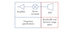
But how does a designer know which process to use for which application? How do we know which process will ultimately result in the best performance for the customer’s particular application? The first step is understanding the application. For example, take a typical signal receiver. It could be the RF subsystem of a smartphone or the front end of an oscilloscope (Fig. 1).
The design requirements of each of the stages shown are unique. At the front end, an amplifier is needed to strengthen weak signals before they are processed. A down-converter or sampler converts high-frequency signals to something that can be digitized. An analog-to-digital converter (ADC) processes the analog or RF signal and creates its digital representation.
Once the design requirements are known, designers can compare the capabilities of various semiconductor processes to select one that is optimized for the application. This is critical because no one technology is ideal for everything. Designers and customers benefit when the best process is used for the right application.
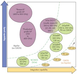
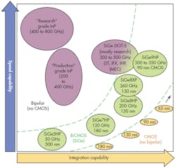
One approach we’ve found useful when comparing technologies is to plot speed capability against integration capability (Fig. 2). In looking at the signal acquisition path of a Tektronix oscilloscope, the compound processes including InP, GaA, and SiGe may be found in the various amplifiers, down-converter samplers, and ADC subsystems that make up a system.
An amplifier may only be a 100- to 500-transistor device, but the transistors need to be fast and precise. A typical CMOS device, on the other extreme, has about a billion transistors in a very small area. You use a few transistors that are very fast when you need bandwidth and low noise and you do the billions when you’re just trying to process 0s and 1s.
As such, CMOS’s strong integration capabilities make it the best choice for applications that involve processing such as visualization, data analysis, or memory interfaces. It should be noted that CMOS is gradually taking over more of the design workload as the technology gets faster, but it will likely never get to the point where it can do everything, and there will always be a need for designers to work in other technologies.
Looking closer at these process technologies, you’ll notice areas of overlap. With continued technology development, we are seeing the advent of new process options that have high integration capability and the speed performance that was previously the exclusive territory of compound processes.
The ability of BiCMOS SiGe to reach higher speeds combined with its integration capability is particularly interesting for scope designers. SiGe also boasts about twice the heat dissipation of InP, which is critical for high-speed applications where a lot of power is needed to handle fast signals. On the flip side, InP has a small advantage in breakdown voltage, but at higher speeds signals are slew-rate limited and rarely if ever reach critical voltage levels where this would come into play.
Another key trend in scopes, most notably in the mid-range, is the growth of more integrated instruments that combine precise signal acquisition with advanced data processing capabilities. The advanced analysis tools help designers address the complexity of embedded designs that incorporate analog, digital, and RF technologies.
In these domains we see similar trends as in consumer devices where designers want to enable functionality and improve performance all at lower cost. Given these constraints, the SiGe BiCMOS process has been a workhorse process, offering an appealing balance of speed and processing power. And as CMOS technology evolves, we are seeing the advanced CMOS nodes considered as replacements for compound processes.
Selecting the right process technology for a given application is a challenging task, and it’s critical to always keep your options open. Technology is constantly changing and evolving, and it’s never safe to assume that the old rules still apply. CMOS is continuing to gain performance while the compound processes are steadily improving in speed. The bottom line for any design team is to build expertise across the board so you can make sure you are giving your customers the best solution possible across your product offerings.
Kevin J. Ilcisin is vice president and chief technology officer at Tektronix. He currently has responsibility for corporate R&D strategy as well as operational responsibilities for technology development. Earlier in his Tektronix career, he held business development and principal scientist roles. Prior to joining Tektronix, he held senior technology and engineering management positions in the laser, display, and semiconductor equipment industries. He was cofounder and VP of engineering of a research and product development firm that contracted with global clients in the consumer display industry as well. He holds PhD and MA degrees in astrophysical sciences from Princeton University. Also, he has a BSc with distinction and the APPEGA Gold Medal in Electrical Engineering from the University of Alberta. He has been awarded more than 40 U.S. patents and has given numerous contributed and invited papers and presentations. He can be reached at [email protected].
About the Author
Kevin Ilcisin
Vice President and Chief Technology Officer
Kevin J. Ilcisin is vice president and chief technology officer at Tektronix. He currently has responsibility for corporate R&D strategy as well as operational responsibilities for technology development. Earlier in his Tektronix career, he held business development and principal scientist roles. Prior to joining Tektronix, he held senior technology and engineering management positions in the laser, display, and semiconductor equipment industries. He was cofounder and VP of engineering of a research and product development firm that contracted with global clients in the consumer display industry as well. He holds PhD and MA degrees in astrophysical sciences from Princeton University. Also, he has a BSc with distinction and the APPEGA Gold Medal in Electrical Engineering from the University of Alberta. He has been awarded more than 40 U.S. patents and has given numerous contributed and invited papers and presentations. He can be reached at [email protected].
Voice Your Opinion!
To join the conversation, and become an exclusive member of Electronic Design, create an account today!

Leaders relevant to this article:


