Silver Nanowires Infuse Flexibility into Consumer-Electronics Design
Two key change-drivers in consumer electronics are enhancing the user experience—product differentiation and relentless cost reduction. When something arrives that allows both of these, it’s a fair bet designers will jump on it fast. Such is the case with silver-nanowire-based touchscreen displays.
This file type includes high resolution graphics and schematics when applicable.
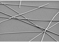
Rarely have the obvious intrinsic values of technology breakthroughs been more clearly defined. In the realm of transparent conductors used in touchscreens, a shift is underway to replace the incumbent material, indium tin oxide (ITO), to electrodes based on silver nanowires (AgNW). The transition in touchscreen technologies, particularly for applications that require screen flexibility and other desired properties, is due to several easily understood differences between the two materials.
The most popular touchscreen technology is projected capacitance, or pro-cap. At the core is a transparent conductor, a layer of material that needs to conduct electricity, yet remain transparent and allow light from the underlying display to shine through the screen. Indium tin oxide (ITO), the legacy conductive material, is neither very conductive nor very transparent compared with AgNW. It’s also too brittle for flexible-display or flexible-touch applications.
Product creators demand conductivity below 100 Ω/square to make their touchscreens more responsive and further improve user experience. Silver is the most conductive material in use. For large-area touchscreens, such as 27-in. monitors, higher conductivity is essential for a fast response time and detection of 10-finger touch.
In laptops and smartphones, film-based transparent conductors can create thinner, lighter, and stronger touchscreens. Higher transmission also enhances battery charge life and/or creates brighter displays, since the AgNW-based touch sensor doesn’t impede light as much as traditional materials. The differing properties of the two most-applied touchscreen materials couldn't be more radical.
For emerging touchscreen applications, including large-area touchscreens, as well as miniature, flexible, wearable displays, silver nanowires offer a significant advantage in both cost and performance. The material is coated on a flexible roll of film that’s a few feet wide and could go a mile in length, using a roll-to-roll process.
Silver nanowires are already being used in several consumer products. Roll-to-roll processed silver-nanowire transparent conductors are the clear choice for new production facilities needing high throughput and easy processing. They're also on target for CE OEMs needing a thin, light, flexible material that delivers high performance for their next killer products.
Enhanced User Experience
In the “touch age,” touchscreens should be thin, light, invisible in various ambient light conditions, and highly responsive. As expectations for low-cost, high-performance products grow, so does demand for higher-quality touchscreens. In particular, fast-responding transparent touchscreens have become essential to a desirable user experience. This can only be achieved with highly transparent conductors not visible to the eye. AgNW is the essential enabler of these key benefits.
In terms of price, silver nanowire-based touchscreens range from slightly less to significantly lower cost than equivalent ITO film-based solutions. Silver nanowires cost less because of three major factors: the capital equipment required to make the product is a fraction of the cost of ITO manufacturing equipment; silver-nanowire-based film can be laser-patterned at room temperature, a process that requires no consumables; finally; and single-layer sensors can be made with silver nanowires that eliminate the need for an additional substrate and adhesive.
Specifying silver-nanowire-based touch technology doesn't have a downside, and offers numerous advantages. The material is cost-effectively accelerating the transition to flexible and wearable devices and products that once only captured the imagination. Forthcoming generations of much smaller or incredibly larger touch interfaces will continue to push the envelope on performance while expecting an even lower price—a trend that silver nanowires are poised to meet.
It’s no secret that wearable electronics is an exploding consumer category. But if designers struggled to make hard, flat products like notebooks, tablets, and phones survive daily wear and tear, wearable products are a whole new game. The good news is that flexibility, a rather desirable feature of things attached to humans, is advancing significantly thanks to a big leap forward in materials.
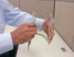
Creating electronic devices for humans means the interface must radically evolve. Brittle glass is out. Flexible electronics and interfaces provide enhanced portability and durability, and allow for virtually unlimited design flexibility. For instance, flexible touch displays enable improved ergonomics, or imagine unbreakable phone screens that flex instead of shattering when dropped or sat on.
Consider folding a 7-in. tablet so that it can slip into your pocket. How about a display that wraps around your arm, or a huge public display or solar cell wrapping around a pillar or a building like a large banner? We are driving toward products like these, which is pushing demand for flexible, bendable, and rollable touchscreens. As more product designers use silver-nanowire touchscreens, we'll be seeing an array of innovative new products.
Transparent conductors may also be applied as electrodes for LCD, OLED, thin-film photovoltaic cells, and other applications not yet conceived of at present. In general, the design requirements remain the same—higher conductivity and improved light transmission.
Market Movement
According to electronics research firm IDTechEx, worldwide shipments of touch-screen panels will double in area from 2014 to 2025. Researchers at IDTechEx reported in part, “...the progress of wearable technology is of increasing interest and focus of developers. It requires the new form factors that printed, organic and flexible electronics can offer for products that can be priced to have reasonable margin.”
Silver nanowires are being adopted as the transparent-conductor-of-choice by leading industry heavyweights such as Hitachi, LG, TPK, Nissha, 3M, Okura, and others. The switch is on and being driven by the range of key factors mentioned above. For product designs that demand higher performance than conventional touchscreens, developers should look into true, single-layer touchscreens and higher-conductivity silver nanowire-based solutions that are ready for wearable, flexible devices—and much more.
This file type includes high resolution graphics and schematics when applicable.
John LeMoncheck is president/CEO of Cambrios Technologies Corp.
About the Author
John LeMoncheck
CEO
John LeMoncheck, CEO of Cambrios, previously served as president and CEO at SiBEAM, a leader in millimeter-wave solutions and developer of high-speed wireless communications technology. Before joining SiBEAM, LeMoncheck was vice president of Consumer Electronics and PC/Display Products for Silicon Image, where he led the company's successful launch and commercialization of the HDMI standard.
An industry veteran, LeMoncheck held executive roles at various technology companies including TeraLogic, subsequently purchased by Zoran and now owned by CSR, Arithmos Inc., which was successfully acquired by STMicroelectronics, and was a member of technical staff at Synaptics. John holds a BSEE from UC-San Diego and spent several years researching VLSI for imaging and pattern recognition applications at Caltech.
Voice Your Opinion!
To join the conversation, and become an exclusive member of Electronic Design, create an account today!

Leaders relevant to this article:


