This file type includes high resolution graphics and schematics when applicable.

Intel co-founder Gordon Moore made the observation in 1965 that the number of transistors per square inch on integrated circuits had doubled every year since the integrated circuit was invented. He also predicted that this trend would continue for the foreseeable future, in what is now commonly referred to as “Moore’s law.” While Moore's law is obviously not a physical law, the rate has generally held steady over the last 50 years. Some people, though, credit that more to the industry’s use of his prediction to actually guide their long-term planning and R&D targets.1
However, since 2012 and the introduction of the 22-nm node, the rate of advancement has slowed. New technology challenges and requirements such as multi-patterning, finFET transistors, and layout-dependent effects have not only forced design and process into a more collaborative space, but also driven the increased use of design-for-manufacturing (DFM) techniques to ensure design quality and manufacturability.2
Reading all of these editorials, blogs, books, etc., one could easily conclude that Moore’s law is coming to an end. But with all of the activity I’m seeing these days at the 20-nm node and below, I’m not so sure. Clearly technical and business challenges must be overcome, but that has been true for every process node since the semiconductor industry began.
Technical and Business Challenges
Admittedly, real challenges emerge when moving to sub-20 nm, both technical and business. At 20 nm and below, there appear to be three key technical challenges: silicon manufacturability (including manufacturing variation), design complexity and size, and concurrent optimization of design objectives (such as power, performance, and area). The business challenges are more economic—fab, process, and design costs. While chip scaling enables the manufacture of smaller devices at lower costs, the increased costs of getting there seems to indicate that fewer companies can afford to be at the “bleeding-edge” nodes.
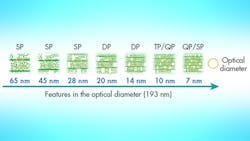
One major technical limitation is the lithography process. With wafer lithography stuck at 193 nm, the optical diameter stays constant. And yet, with no change in exposure wavelength, the features we all need to design and manufacture continue to shrink in size and pitch (Fig. 1). As a result, more lithography/process/design tricks are needed to reduce feature size and pitch.
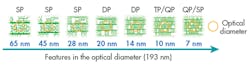
For example, we had to move from single patterning to double patterning (DP) at 20/16/14 nm. The 10-nm level will bring triple patterning, (TP), quadruple patterning (QP), and variants of spacer-assisted double patterning (SADP). While extreme ultraviolet (EUV) lithography continues to be the hope to reduce the need for multi-patterning, it looks less and less likely to intercept 7 nm, so no short-term help there.
Further complicating the situation, with a constant optical diameter, more and more features interact with each other. At 65 nm, the optical diameter was on the order of a single cell height; today, it covers many cells/tracks. The context around any given pattern has become more and more important to manufacturability and performance, driving more complex design rules and the rapid growth of pattern matching used in both design and manufacturing—a story for another article.
On the business side, wafer costs have always increased node over node, driven by increases in manufacturing costs. For the last 30 or so years, we enjoyed lower cost per transistor node over node until 20/16/14 nm, where the increased manufacturing cost was high enough that the increased transistors/area didn’t offset the higher cost. Are we done, then? No, 10 nm looks like a node at which the cost per transistor will again show improvement. Because of this, 10 nm will likely be a very attractive node with a long life.
So, what is the take-away here? Sub-20-nm nodes are harder technically, but the next technology node has always been harder. Two nodes out, things have always looked impossible. Creative people solved the technical issues, and we continued down Moore’s law. That was just as true back at the 1-µm (1000 nm) node as it is today at 10 nm.
What is the Market Really Doing?
In a nutshell, I’m seeing an enormous amount of aggressive drive by a somewhat surprisingly large number of companies moving to sub-20-nm nodes. International Business Strategies Inc. (a well-respected and generally accurate analysis company) stated in a recent report that “…only a small number of IC vendors are implementing highly complex designs at advanced technology nodes, and these include Intel, Qualcomm, Broadcom, Avago, Samsung, HiSilicon, nVidia, AMD, Xilinx, Altera, MediaTek and Cavium.” They also go on to list Apple and ARM.3 And they are far from being alone in this belief.
In fact, the reality is far rosier than the critics would have you believe. My team has been working with more than 75 IC, foundry, and IP companies using Calibre tools for DRC/MP sign-off at 20 nm and below—a number that continues to grow every quarter. Volume production at 20 nm has been going on for basically one year, and 16/14 nm entered volume production this year.
Given these facts, I find 75+ companies and growing a strong indication that, rather than shying away from sub-20 nm, the industry is moving ahead. Similarly, I have seen half-a-dozen companies already working on 10-nm test chips, and they will be moving to risk production in the first half of next year. Oh, and the first Calibre DRC/MP rule decks are already available for strategic customers to start their initial 7-nm development.
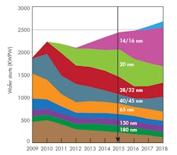
So we have lots of design activity, but is it turning into chips? Clearly, yes, as you can see by looking at the wafer start graph (Fig. 2). Approximately 40% of the wafer starts in 2015 are 20 nm and below.
Conclusions
We have reached a unique moment in time. We are ramping two volume production nodes (20 and 16/14 nm), entering risk production (10 nm) on a third node, and starting development on a fourth (7 nm). I cannot remember a time when there was so much overlap between technology nodes ramping up at the same time. Further, all of these nodes have been criticized for being too expensive, too difficult to design (due to multi-patterning, etc.), leading to the “Is Moore’s Law dying?” discussion in the media.
Technical challenges always need to be solved at the next node. This creative industry has solved them, time after time. Business challenges must be solved at sub-20 nm, too. But with the breadth of companies moving to these nodes, folks are addressing these challenges and aggressively moving forward. Is Moore’s Law dying? I’m not seeing it.
References:
1. Disco, Cornelius; van der Meulen, Barend (1998), Getting new technologies together. New York: Walter de Gruyter. pp. 206–207. ISBN 3-11-015630-X.
2. “Top Five Design and Manufacturing Challenges at 20nm,” Semiconductor Manufacturing & Design. March 21, 2012.
3. “Global IC Industry System Service Report – Design Activity,” July 2015, International Business Strategies Inc.
About the Author
Michael White
Michael White is Director of Product Marketing for Mentor Graphics’ Calibre Physical Verification products. Before joining Mentor Graphics, he held various product marketing, strategic marketing and program management roles for Applied Materials, Etec Systems and the Lockheed Skunk Works. Michael received a BS in System Engineering from Harvey Mudd College. He also holds a MBA/BS in engineering management from the University of Southern California.
Comment About the Article
To join the conversation, and become an exclusive member of Electronic Design, create an account today!

Leaders relevant to this article: