11 Myths About High-Level-Synthesis Techniques for Programming FPGAs
Download this article in PDF format.
The numbers of applications using FPGAs are on the rise. They have long been used for avionics and DSP-based applications, but are finding many new applications in which their flexible and configurable compute capabilities are much in demand. These applications include accelerating large compute-intensive workloads, within wireless base control and management functions, and already look set to play a major role in vision processing in autonomous driving systems.
Their strength comes from the fact hardware developers can program it to deliver exactly what they need for their design. When they were students, many engineers might have learned that they can program FPGAs through the use of a hardware description language (HDL), the most popular of those being VHDL and Verilog.
An HDL is used to implement a register-transfer-level (RTL) abstraction of a design. In time, the process of creating RTL abstractions was made easier through the use of reusable IP blocks, speeding the design-flow process. As designs became more complex and the time-to-market pressures increased, developers and the vendor community have strived to provide more software-based tool chains to help reduce development times.
One of these techniques is “high level synthesis” (HLS). HLS can be thought of as a productivity tool for hardware designs. It typically uses C/C++ source files to generate RTL that is, in most cases, optimized for a particular target FPGA device.
Like many new ways of performing a task, a number of myths have evolved surrounding HLS. Let’s review them and understand how some of them have come about.
1. Results achieved with HLS aren’t as high quality as those obtained through other means.
So the fact is that you’re relying on the tool to give you RTL, from which you will benefit from a large gain in productivity; getting more RTL in a given period of time. The alternative is very similar to coding a microcontroller in assembly language. Yes, you could do that, and most probably you’d achieve a more efficient code. But does anybody do that now apart from in very specific cases?
The goal of using an HLS tool is to be within 10-15% of what you could achieve by hand coding. There’s an added bonus to HLS tools that are provided, often for free, from the FPGA vendor—they’re most likely heavily optimized to suit the device. Only the vendor will have the inside knowledge to make the best use of architecture and routing. Thus, the resultant RTL has the target hardware knowledge factored in from scratch.
HLS tools typically include an aspect of design exploration that allows you to tailor the implementation to match the resources of the target device. There’s no doubt that an experienced RTL designer could get a more optimal architecture, but an HLS optimized for the device can provide optimal results in the shortest time.
2. HLS tools have long learning curves.
Any new tool involves a learning curve. If you’ve been working with RTL for 20 years, then you’ll be very familiar with RTL—learning a new approach will take some time, but it’s measured in weeks rather than months. Many books have been written on HLS, plus there’s a lot of excellent online training, some of which comes from leading universities. On top of that, the tools themselves ship with tutorials, not to mention continued online training provided by the vendors themselves. For example, Intel HLS ships with 10 tutorials.
3. HLS is an early adopter technology.
The opposite is actually true. Mentor Graphics, for example, launched its Catapult tool some 16 years ago. HLS is a mature technology, with the FPGA industry having driven the approach to making it mainstream with cost-free, high-quality design tools.
4. I need to use HLS for my entire design.
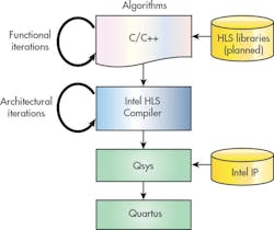
This is another myth that needs to be dispelled, since HLS complements the standard FPGA design-flow process. FPGA vendors all provide a lot of designs and IP. Therefore, the time you might be using HLS could account for just those parts of a development that need some degree of “secret sauce” when you’re perhaps developing complex algorithms for designs such as data centers, wireless communication, vision processing, and avionics. Across the industry, a rich portfolio of IP is available that perfectly complements using HLS.
Intel FPGA programming tools include the HLS Compiler. It works with Intel’s Qsys integration tool and Quartus design software.
5. I need to be a software developer to use HLS.
The reason why this is a myth is that HLS is a hardware-design productivity tool. You certainly need to be able to code in C/C++, which for most hardware designers is manageable. The code needs to impart or imply the heart of the architecture, and you can be abstract in the coding as long as it infers the hardware architecture, memory, and data flow that you wish to achieve.
You don’t actually need to code every last detail, so a block diagram approach would really help. In many ways, a software developer might actually struggle using HLS, since they probably wouldn’t have the required depth of hardware design knowledge.
6. HLS breaks my verification flow.
An RTL designer will commonly use a testbench to verify the design. Most would place the RTL code back into the C model to verify that the RTL achieves what the architecture implied in the C code. It doesn’t matter whether this RTL was generated through VHDL/Verilog or by HLS; both can be verified back original model.
7. HLS doesn’t support multi-rate DSP designs.
Very common in communication and radar systems, there are a number of requirements, for example, when down-sampling the data rate. A number of well-documented HLS methods support multi-rate DSP designs, including polyphase decimation or polyphase interpolation filtering. So, yes, HLS does support multi-rate DSP designs.
8. HLS may not support my interface requirements.
Not the case. Concerns regarding getting data in and out of a design are unfounded. High-level-synthesis techniques use pragmas that allow the developer to specify the standards required by the interface. Supporting memory maps, streaming, and wired interfaces, it allows you to customize the interfaces to your system requirements.
9. No IP is available for HLS.
As you may have gathered from some of the above points, there is indeed a lot of IP available. Some of the IP is available as libraries for vision, DSP, and math functions. Much like with C programming, extensive math functions and a growing list of available third-party libraries are available for use with HLS tools. In fact, many of the libraries supplied by FPGA vendors are optimized for their device targets.
10. HLS tools are expensive.
No, not the case. The FPGA industry is making these tools available at no cost as part of their standard software suites.
11. HLS doesn’t help address challenges of design reuse.
Sorry, but another myth that’s false. HLS helps design reuse because the source code is technology-independent, meaning that the source can be recompiled using different design exploration parameters to suit different target devices.
For example, with a low-cost, slower FPGA device, you might need to use more parallelism within the design to achieve the performance target. However, the next design might mean you can reuse the IP on a higher-performance device; therefore, you could use less device resources. This approach will actually improve design reuse.


