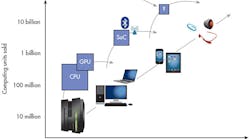
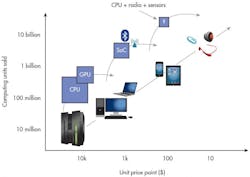
In a conversation with The Atlantic in 2013, outgoing Intel CEO Paul Otellini shared his thoughts on the evolution of the semiconductor industry.1 During the interview, he sketched out the “history of the computer industry in one chart.” Advances in computing have driven the growth of the semiconductor industry in general and Intel in particular.
Indeed, this one chart succinctly illustrates how the increasing ubiquity and pervasiveness of computing has driven down the cost structure of the semiconductor industry over decades. Otellini noted that an aggressive drop in the price per unit has enabled the equally exponential increase in the number of computing units sold over time.
Starting from mainframes that cost tens of thousands of dollars each and shipped only in thousands of units per year, the industry evolved to shipping well over 300 million PC units at less than $1000 per unit. Smartphones and tablets are on track to ship well over 3 billion units at less than $100 per unit. As is evident in market trends, we are on the cusp of a new wave that will further proliferate the ubiquity of computing by shipping over 30 billion units at less than $10 per unit (see the figure).
Known as the Internet of Things (IoT), this new wave of computing will be powered by ultra-cheap, ultra-low-power, and highly integrated chips connected to a cloud or a network and embedded in virtually every physical object around us. Many analysts expect this market to range well over 20 billion units by the end of the decade.2
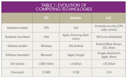
The semiconductor industry has enabled successive waves of computing by re-architecting silicon technology for each wave. Companies that have embraced the new architecture early have been able to support the aggressive reduction in price point and establish leadership. On the other hand, incumbents that have failed to quickly adapt have lost ground to disruptors and have struggled to recover. This observation also holds true in the software industry, where a re-architecting of the operating system (OS) and application software has enabled each wave of computing (Table 1).
For the first time in the history of the semiconductor industry, the next wave of computing will not be driven by the most advanced transistor node, but instead by a lagging transistor node. “Energy-per-operation” will increasingly become the driving metric for the industry, and chip and system-level integration will become the key enablers. Emerging trends, though, are likely to enable the semiconductor industry to support a $10 unit price point for the next wave of computing.
This file type includes high resolution graphics and schematics when applicable.
Transition 1: Mainframe to PC ($1000 Price Point)
The first transition occurred in the early 1980s with the development of a very simple single-chip central processing unit (CPU), Intel’s 80286. Operating at just 6 MHz, it continued to be enhanced over three decades through aggressive transistor scaling and a relentless focus on increasing performance (frequency).
Gradually, additional chips such as the graphics processing unit (GPU), memory, and connectivity were added to the system to increase functionality. The CPU-driven hardware ecosystem complemented a mainstream software ecosystem (initially MS-DOS and eventually Windows) and enabled computing on a mass scale (more than 300 million units) with a price point of less than $1000 per unit.
The combination of the CPU and added chips delivered higher performance and more functionality. The CPU and system architecture were designed for performance. Power was a secondary metric. Intel dominated this wave through an aggressive pursuit of Moore’s Law and the predominance of x86 architecture while Microsoft dominated through a virtual monopoly of Windows in the software ecosystem.
Transition 2: PC to Mobile ($100 Price Point)
The consolidation of functionality on a single chip (SoC) enabled the emergence of the smartphone in the late 2000s. The smartphone and tablet deliver desktop-class functionality with a chipset comprising far fewer chips. This wave of computing established the dominance of the SoC and connectivity solutions and delivered even smaller form factors within a much lower power envelope and much lower cost.
The proliferation of mobile computing was also enabled by dramatically cheaper (eventually free) software ecosystems such as iOS (Apple) and Android (Google) that were specifically designed for mobile (SoC) hardware and not for legacy PC (CPU) hardware. Companies like Apple and Qualcomm dominated the early rise of this wave through the aggressive pursuit of chip-level integration, and the SoC emerged the clear winner over the standalone CPU.
Transistor scaling and Moore’s Law helped further enhance the mobile wave by enabling better SoCs and a more compact SoC solution.3 Companies like MediaTek are driving hard to dominate the maturing mobile wave by offering the entire SoC for under $5 and enabling a unit price point of $100 per unit.
Transition 3: Mobile to IoT ($10 Price Point)
Trends suggest that every tenfold increase in unit volume has been enabled by a tenfold reduction in unit price. So what is the right system/chip architecture to enable greater than 30 billion units at a $10 price point? The answer may lie in even higher levels of on-chip integration.
To support the very small form factors and aggressively low power envelopes required for sensor hubs, many system-level functionalities will need to be integrated on a single chip or package, eventually leading to a system-in-package (SiP) or computer-on-chip (CoC). This trend is already evident based on the basic requirements of an IoT chip.
For example, a generic wearable chip may need to deliver a combination of logic computing (CPU), connectivity (radio/bluetooth/GPS), non-volatile memory (flash), and various analog and mixed-signal functions as well as a variety of sensors. The critical technology metric for such an IoT platform will be its total power envelope, which will need to be as much as 10 times lower than that for a mobile SoC platform.
Semiconductor companies looking to establish leadership in the IoT will need to focus their efforts on functional integration far more than transistor scaling. Several companies are trying to establish early leadership in this space, including a combination of fabless and fab-lite (Qualcomm, Broadcom, Apple, Texas Instruments, STMicroelectronics, NXP Semiconductors), integrated device manufacturers or IDMs (Samsung, Intel), and microelectromechanical-systems or MEMS (STMicroelectronics, Texas Instruments, InvenSense). Foundries too will need to rapidly adapt their transistor technology roadmaps to enable a silicon ecosystem that will enable such integration.
In addition to a new silicon architecture and ecosystem, IoT computing will rely on cheap, widely available standard software that will enable the hardware to communicate with each other and to the cloud while allowing an independent and robust developer ecosystem to proliferate. Qualcomm is attempting to take an early lead in this space with AllJoyn while Samsung is promoting its Tizen OS. Google recently released Android Wear for developers in the wearable space. Many others are establishing leadership in this emerging market.
Transistor Platform for IoT Computing
IoT broadly describes the entire emerging segment of connected and pervasive computing systems and platforms. These systems will have wide-ranging technology requirements depending on the end application.
Cloud computing and datacenters will form the back end of the platform and serve as the repository of all the data generated by a vast array of connected applications, including consumer, industrial, medical, and environmental, which will form the front end. The front-end devices will in turn have a wide range of performance and power requirements.
Wearable technologies such as Google Glass represent a category of devices that heavily utilize imaging and video and will need high-performance (multicore, gigahertz frequency) and low power. Fitness trackers such as Fitbit and Jawbone’s UP represent a category of devices that employ location sensing, motion sensing, and modest (less than 100 MHz) computing. A little sensor that records data in a remote oil field and sends it to the cloud may not need much compute power, but it will need extremely low standby power and very long battery life in addition to extreme temperature stability.
Regardless of the end application, the focus of transistor development over time will shift from “performance-per-watt” to “energy-per-operation.” Many of the sensing platforms and devices that will become part of the IoT will need to have battery life on the order of months or years (e.g., remote infrastructure monitoring). Many more will require battery life on the order of weeks or months (e.g., wearable technologies). And yet many more will harvest or scavenge energy and run on no battery at all (e.g., medical patches).
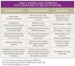
Many of these applications are likely to be single use and replaced upon battery discharge. Since many of them must be off or in a standby state while retaining a sizable amount of data, ultra-low standby power is crucial in addition to low active power. An ideal IoT platform will be able to meet these attributes and provide designers the flexibility to incorporate any combination of them on a single chip (Table 2).
A transistor platform that supports these specifications at the lowest system cost will win in the IoT/wearables space. Unlike CPU technology, the transistors that make up this platform are not limited by geometrical (pitch) scaling. For example, analog and high-voltage (2.5/3.3 V) blocks have not been scaled over several logic technology generations due to very stringent requirements on variability matching.
The most advanced embedded non-volatile memory (eNVM) technology in production today uses design rules that are four times larger than the most advanced logic technology. As a result, chips that are dominated by analog/eNVM do not benefit from the geometrical scaling of logic transistor densities.
Based on these requirements, 40/45/55/65-nm technologies are best suited to support the bulk of the front-end IoT and more specifically the wearable technologies space in the near term (two to three years). The Newton platform by Ingenic Semiconductor is one such integrated computer-on-a-chip.4
Applications like Google Glass that require higher performance and can accommodate the higher cost will use 28-nm technology right away. Three to five years out, the high-end IoT space likely will continue to be served by 28-nm planar transistor technology while the bulk of the IoT space will utilize 40-nm technology, provided a suitable eNVM solution can be developed by then.
Given the requirements of cost, power, and functional integration, it is unlikely that sub-20-nm transistor technology will serve the mainstream IoT or wearable technologies space for another five to seven years, if ever. Once a starting technology is in place for such applications, an enhancement roadmap will be driven not so much by geometric scaling, but more by aggressively lowering the power envelope and integration of more functionality.
Foundry IoT Transistor Roadmap
Through most of the CPU era, semiconductor R&D programs were driven by a performance-centric roadmap. The roadmap began to emphasize more on-chip integration during the SoC era. The foundry roadmap during the IoT era will be driven by overall power reduction and even higher levels of on-chip integration.
With every successive wave of computing, increasingly more value was extracted from silicon while driving down its overall contribution to the unit bill of materials (BOM). This trend will continue and will move the industry to deliver the “same performance for less cost” or “same power for less cost.”
“More than Moore” is used to describe orthogonal scaling as opposed to geometrical scaling of Moore’s Law. For example, orthogonal scaling rejuvenates a legacy technology to reduce its total power envelope. Such innovation may also be extended to include enhanced on-chip functionality such as eNVM or enhanced system-level functionality via 2.5D scaling (interposers) or 3D scaling (through-silicon vias, or TSVs).
Judicious investment in these areas will enable foundries to capture a significant projected silicon volume migrating from 130 nm to 28 nm over the remainder of this decade. Continued Moore’s Law scaling is likely to serve a limited number of applications and may not lead to high-volume design wins in the IoT space, at least in the near term. Whether very advanced transistor technologies (sub-20 nm) can offer the most effective integrated platforms necessary to succeed in this space is still to be determined.
For the first time in the history of the semiconductor industry, a lagging transistor node will drive the next wave of computing, not the most advanced transistor node. A holistic platform and system-level view suggests that cost, power, and highly disparate functional integration are the key technology metrics for success in the emerging wave of computing.
This file type includes high resolution graphics and schematics when applicable.
References
1. “Paul Otellini’s Intel: Can the Company That Built the Future Survive It?” Alexis C. Madrigal, The Atlantic, www.theatlantic.com/technology/archive/2013/05/paul-otellinis-intel-can-the-company-that-built-the-future-survive-it/275825/
2. “Gartner Says the Internet of Things Installed Base Will Grow to 26 Billion Units By 2020,” www.gartner.com/newsroom/id/2636073
3. “System-on-chip technology comes of age,” Pushkar Ranade, www.eetimes.com/document.asp?doc_id=1279975
4. “Newton is the first MIPS-based mini-computer for wearables,” Agam Shah, PCWorld,
www.pcworld.com/article/2138640/newton-is-the-first-mipsbased-minicomputer-for-wearables.html


