The sheer range of FPGA applications has led to the development of an array of different devices, each with individual strengths and weaknesses. It has never been more important to know your FPGA.
Related Articles
- An FPGA "Companion" In Smart-Phone Design
- Understanding FPGA Processor Interconnects
- Expanding The FPGA Interconnect
The first FPGAs to arrive on the market had a relatively simple architecture. They employed static random access memory (SRAM) cells as their circuit-configuration and lookup-table (LUT) elements.
The LUT, most often a four-input, single-output element, is the core logic element of many FPGAs on the market. Together with programmable routing, it provides the device with flexibility and scalability. The LUT also allows arbitrary truth tables to be built in each FPGA, providing the basis for complex logic functions that can be reprogrammed as requirements change.
The SRAM memory elements used in most FPGAs are volatile. The configuration and LUT contents are lost when the system is powered down. As a result, the devices are designed to automatically retrieve the configuration from non-volatile memory upon device power-up. This reconfigurability can be leveraged in designs that need high flexibility at runtime.
More and more devices support partial reconfiguration to allow different hardware configurations to be uploaded on the fly. In practice, partial reconfiguration can be used to upgrade portions of the FPGA while the rest of the system stays up and running or to optimize the use of programmable logic cells within the FPGA fabric.
Partial reconfiguration has proven popular in fields such as audio and video signal processing since it permits hardware-accelerated algorithms to be tuned to the incoming stream of data. This means that a smaller device can be used to support the full range of required system tasks by reconfiguring modular circuits, set within an area of the fabric. If partial reconfiguration were not used, each circuit would need to be loaded into a larger fixed-configuration device in parallel, requiring more fabric resources.
Antifuse FPGAs
Not all FPGAs use volatile memory for configuration. The first non-volatile devices were based on antifuse technology, a one-time programmable element that forms a connection when the fuse is “blown” electronically by an external programmer.
Antifuse FPGAs have greater natural immunity to high-energy radiation than memory-based devices, as the permanent connection formed by the antifuse cannot be altered by single-event upsets. As an example, Microsemi has a reprogrammable non-volatile option in the form of its SmartFusion, ProAsic3, and Igloo series of FPGAs (Fig 1).
These devices combine a LUT-based architecture with configuration cells built on flash-memory technology. The entire system then can shut down but still provide for immediate power-up because the FPGA fabric preserves its configuration state. This also eliminates inrush configuration current and saves energy when the device power source is cycled.
Unlike antifuse technology, the flash memory cells are reprogrammable. If a mistake is made during development, or the system needs to be upgraded in the field, the devices’ hardware configuration can be altered.
Flash Memory
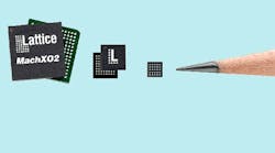
Flash memory has enabled hybrid architectures and provided features such as enhanced security. Lattice Semiconductor’s MachXO2, for example, has its own on-chip flash storage for configuration data, reducing the risk of hackers tapping into and recovering the configuration bit-stream during power-up (Fig. 2). This feature removes the need for an external configuration PROM.
The flash contents of the MachXO2 can be loaded into SRAM across a very wide internal bus, enabling a power-up time within 1 ms. An additional area of on-chip flash lets designers use the memory for non-volatile data storage, reducing the need for external memories.
The first FPGAs almost completely comprised purely “soft” logic, strictly fabric with no ASIC-gate based blocks. As FPGA applications have widened, with an increased demand for technology in areas such as communications and signal processing, manufacturers have added higher-performance dedicated logic blocks to more efficiently use die area. One of the most common elements is the serialiser/deserialiser (SERDES) interface. The SERDES block is now included in many FPGA architectures.
The power consumption of I/O has become a critical challenge in system design. Although sending data in parallel can offer high bandwidth, the use of multiple data lines sending bits simultaneously can demand a lot of energy and present signal-integrity challenges, particularly as clock speeds increase.
Serial I/O can offer better signal integrity at high bitrates through the use of adaptive equalisation and other signal-conditioning techniques. As they typically use low-voltage-swing logic levels, serial interfaces can improve power efficiency. As a result, serial channels are now used widely for high-speed memory interfaces as well as chip-to-chip and board-to-board communications.
Serial I/O
Serial I/O requires the support of relatively complex logic blocks that would be costly to implement purely in programmable logic. Dedicated SERDES logic blocks based on “hard” ASIC gates allow for quicker signal transmission and a higher-speed circuit.
Logic is needed to convert the signals that come from an internal parallel bus into a clocked serial representation and recover the data from an incoming serial link. By offering this kind of SERDES function in dedicated hardware, today’s FPGAs enable more of the programmable logic to be used for the end application.
SERDES blocks are common in many of the mid-grade and all of the high-end FPGA families. The Altera Stratix, Lattice ECP3, and Xilinx Virtex devices all provide SERDES blocks. Some of these FPGAs support serial data rates up to 28 Gbits/s using a combination of signal-conditioning techniques.
Cost-optimised FPGAs such as the Altera Cyclone, Lattice MachXO2, Microsemi SoC Igloo, and Xilinx Spartan families often provide support for low-voltage signalling interfaces such as low-voltage differential signalling (LVDS), but largely leave the implementation of the SERDES functionality to programmable-logic blocks.
Dedicated Communications Cores
Dedicated communications and utility cores appear on cost-optimised FPGAs to allow their use in higher-volume industrial and consumer applications. For example, Lattice’s MachXO2 family includes hardened functions such as I2C and SPI ports as well as timers and counters, providing similar functions to those found in off-the-shelf microcontrollers but with the much greater flexibility of uncommitted logic in the rest of the array.
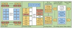
Microsemi’s SmartFusion is a hybrid FPGA, analog, and microcontroller architecture that combines a complete ASIC-gate based ARM Cortex-M3 processor core and analog compute engine (ACE) with an FPGA fabric. The hybrid architecture lets the developer run software within the ARM supported by custom peripherals loaded into the FPGA’s fabric.
The SmartFusion architecture also includes an intelligent I/O controller that optimises the performance of sensor-oriented applications. Integrated analogue I/O blocks, under the control of the ACE, ensure offloading of the processor for parallelising system operations.
Signal Processing
As FPGA signal-processing applications increased, vendors began to add hardened blocks based on ASIC gates for high-speed arithmetic. The most efficient way to implement multiplication in programmable cells is to use bit-serial arithmetic. However, this approach is very slow and only provides benefits if many arithmetic operations can be performed in parallel.
The first step beyond bit-serial arithmetic was to add dedicated carry-chain logic, which is expensive to implement in the FPGA’s fabric. This allowed the use of much faster carry-lookahead and carry-save adders, both of which allow the implementation of faster multipliers.
The next step was to provide complete multiplier blocks in hardwired logic. These blocks can be quite narrow to reduce their die consumption, but they easily can be tied together to form more sophisticated 32-bit and 64-bit multipliers, using the FPGA’s fabric to add support for more sophisticated features such as floating-point arithmetic.
Some FPGAs provide a variety of DSP cores to suit target applications, with multiple narrower 9-bit units, favoured for image and video processing, and wider cores used for audio and communications signals.
DSP blocks appeared first in the high-end devices, but have now migrated to cost-optimised architectures such as the Cyclone V and Spartan-6. For applications where the arithmetic processing does not suit standard arithmetic operations, such as cryptography or specialised video operations, an architecture that has a higher ratio of programmable logic to DSP cores may be a better choice.
One thing is for certain—there is an FPGA that is well suited to your application. A distributor with experience and knowledge of these options is ideally placed to help you get to know your FPGA.


