For the most part, embedded FPGA can be viewed as a “black box,” which is effectively as an RTL engine. However, sometimes it’s helpful to understand what’s going on underneath the hood to evaluate applications and competitive alternatives. This article will provide a close-up view and discuss how embedded FPGA works in general.
What is an Embedded FPGA?
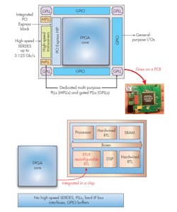
An embedded FPGA is an IP block that allows a complete FPGA to be incorporated in an SoC or any kind of integrated circuit (Fig. 1). While embedded FPGA is new, the idea of what used to be chips becoming IP blocks is old. For example, RAM, SERDES, PLL, and processors are all routine IP blocks today that were once standalone chips. Now FPGA is an IP block, too.
1. An embedded FPGA IP core is similar to the core on an FPGA chip.
Conceptually, it seems as simple as using the core of an existing FPGA chip, but as you’ll see, it’s really not that simple.
An FPGA is an Array of Programmable Logic
The basic building block in every FPGA is the lookup table (LUT). Different FPGAs use different-sized LUTs, but they all use some sort of LUT. A lookup table is equivalent to a RAM with the inputs being the address select lines. Since a 4-input LUT with one output has 16 possible input states, it requires 16 configuration bits that can be programmed to implement any Boolean function. The LUT can be 5-input or 6-input or any number of inputs: 2^N configuration bits are required. A LUT can also have multiple outputs so that there are two Boolean functions of the same inputs (this doubles the number of configuration bits).
To cite a particular example, we’ll use the Flex Logix embedded FPGA platform called EFLX, since that platform has the most public information available on its website. In the second generation (Gen2) of EFLX, the LUTs are 6-input with dual outputs, and it’s configured so that it can be used as dual 5-input LUTs or a single 6-input LUT (Fig. 2).

