MCUs Combine Low Power, DSP Functionality in IoT Edge-Node Apps
Download this article in .PDF format
The Internet of Things (IoT) is already bringing big changes to many aspects of life. During the daily commute, a GPS-equipped smartphone determines when the driver is 30 minutes away and tells a smart thermostat at home to turn on the air conditioning. An industrial machine gathers real-time data from vibration sensors and transmits it to the cloud to predict failures before they can interrupt production. In healthcare, an instrumented adhesive patch can help a remote medical team monitor a patient’s vital signs.
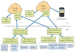
These requirements are changing the way designers build IoT systems. They must accommodate two conflicting requirements: boost processing capability and simultaneously reduce power consumption (Fig. 1).
In the traditional IoT model, the local, or edge, node captures the data from its sensors and passes it to a higher level, typically the cloud, for processing, analysis, and action. Though an effective approach, it’s now becoming a victim of its own success.The Trouble With Tribbles Data
Market-research firm IDC estimates that 50 billion machines will be connected to the internet by 2020. As applications proliferate, the amount of data that must be processed increases dramatically—for example, each meter in the smart grid produces 35 GB of data per day, and each blade of a gas turbine can generate up to 500 GB per day.
Just as the Tribbles’ uncontrolled breeding overwhelmed the crew of the U.S.S. Enterprise in Star Trek, this vast increase in data puts immense strain on the communications infrastructure. It slows system response or forces an upgrade to faster, more power-hungry networks.
Consequently, designers are pushing processing from the cloud to the node wherever possible. As the functions performed by a node become more complex, the node-level microcontroller must increase in capability.
A typical list of tasks assigned to the node microcontroller might be:
1. Acquire the node data, either directly from the sensor(s) with an analog-to-digital converter (ADC), or indirectly via a wired or wireless connection.
2. Extract the desired information from the data using signal processing in the digital domain.
3. Perform post-processing actions on the information. For example, the microcontroller can close the loop locally and control a valve or other actuator, perform local diagnostics, transmit the information to a local gateway or the cloud, and more.
4. Relay information from other nodes as part of a mesh network, or perform other tasks as part of an intermediate-level control loop.
Low Power Consumption and the Hardware Accelerator
Another requirement is in direct opposition to the need for more edge-node processing power: low power consumption. For many remotely located nodes, it’s either not feasible or very expensive to add wired power, so they rely on batteries, solar power, or other low-capacity sources.
As a result, a microcontroller in an edge node typically spends much of its time in a low-power sleep mode, only waking up when needed to respond to a message or process data from a sensor. To conserve battery life, it’s important to minimize the power consumption during the wakeup phase. Thus, the microcontroller must perform its functions as efficiently as possible.
A low-power MCU is essential, but the DSP tasks outlined above require something more: a co-processor, or hardware accelerator, optimized to perform the tasks needed for DSP operations.
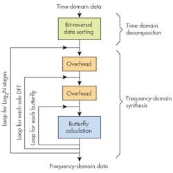
Why use hardware rather than software for this job? The algorithms employed to implement DSP functions typically require the repeated execution of multiple mathematical operations on a series of data samples. Fig. 2 shows one such function, the fast Fourier transform (FFT), which converts data from the time domain to the frequency domain and vice versa.
It’s possible to perform these DSP operations in software, of course, using a high-level language such as C, but this is computationally demanding and relatively slow. A hardware accelerator implements an architecture that’s optimized for repetitive manipulation of data sets, so that it extends the amount of time the microcontroller can spend in low-power modes. This conserves energy while improving signal-processing performance.
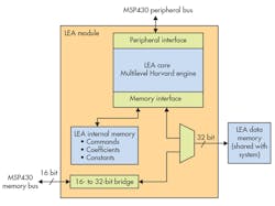
The low-energy accelerator (LEA) in the MSP430 microcontroller family, for example, is a 32-bit vector math engine that performs DSP operations in an energy-efficient manner. The LEA is able to perform without any CPU intervention; it triggers an interrupt upon completion of a task.
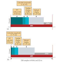
Figure 3 compares the performance on a 256-point FFT of the MSP430 running a traditional C implementation versus the MSP430 with the LEA enabled. The accelerator reduces the FFT processing time by 93%, from 9.64 ms to 700 µs.
Software Tools
Most engineers designing IoT nodes are not DSP experts, so it’s important to have a comprehensive set of software tools with ready-made code for common DSP operations. Using these tools saves development time and provides a level of abstraction from the hardware.
Texas Instruments offers a DSP library that includes highly optimized functions to perform many common operations on fixed-point numbers, including the Multiply and Accumulate; the FFT discussed earlier; the finite-impulse-response (FIR) digital filter; and the infinite-impulse-response (IIR) filter.
It’s available for the MSP430 and MSP432 MCUs (either with or without the LEA block), and runs under the Code Composer Studio Integrated Development Environment (IDE).
About the MSP43x Family
Texas Instruments’ low-power MSP43x family of microcontrollers combines high performance and low power consumption for edge-node applications. The family has more than 500 members, including the MPS430 ultra-low-power (ULP) versions based on a 16-bit RISC core, and the MSP432 based around a 32-bit ARM Cortex-M4F that combines low power plus performance.
The MSP430FRxx set of 100 devices feature ferroelectric random access memory (FRAM) technology for unique performance advantages. FRAM combines features of both flash and SRAM technologies. It’s non-volatile like flash memory, but FRAM offers fast and low-power write performance, a write endurance of 1015 cycles, improved code and data security, and high resistance to electromagnetic fields and radiation.
One series of devices in the FRAM group, the MSP430FR599x, is the first to include the LEA. The series includes the MSP430FR5992 and the MSP430FR5994, with 128 kB and 256 kB of FRAM, respectively.
LEA Operation in the MSP430FR599x
The LEA itself isn’t directly accessible, but its operations may be accessed via the MSP DSP Library. The MSP430 family has a 16-bit RISC core, so the LEA architecture (Fig. 4) includes a 16- to 32-bit bridge.
The accelerator operates based on the commands provided to it during configuration. These commands are pointers to the type of operation and memory input or output buffers.
The MSP430FR599x MCU has a total of 8 kB of static RAM (SRAM)—4 kB are shared with the LEA for data input, output, and parameters such as coefficients and constants. Before using the Library APIs, the user must first specify the input and output memory locations as an array within the shared 4-kB SRAM. In a 256-point complex FFT, for example, the data input array consists of 512 words (1024 bytes), comprising 256 words each of real and complex values.
Below is a sample sequence of operations for a vector-based algorithm using the LEA. The sequence makes use of other MSP functional blocks: DMA (direct memory access); a 12-bit ADC; and SPI (serial peripheral interface):
1. The CPU initializes the DMA controller, ADC, and SPI blocks.
2. The selected DMA channel collects ADC samples at the defined sampling rate and transfers the data to the LEA memory.
3. After a block of data is collected, the CPU enables one operation, or a series of operations, of the LEA using the APIs in the DSP Library to execute the required algorithm.
4. When the algorithm is complete, another DMA channel transfers the results to the SPI.
5. The SPI transfers the data to an external device.
A signal-processing and reference design is available that demonstrates the LEA’s performance on filtering and signal-processing functions. The reference design uses TI’s LaunchPad and BoosterPack system to benchmark LEA performance gains that can be readily applied to IoT applications such as flow metering, industrial sensing, and portable health monitoring.
Conclusion
As the amount of data gathered by IoT applications continues to increase, a combination of local processing and low energy consumption is a prime requirement for edge-node designers.
The LEA allows the MSP430FR599x to achieve 40X the performance of standard ARM Cortex-M0 microcontrollers on DSP operations while still consuming only 120 µA/MHz in active mode. The combination of high performance and low power consumption is well-suited for the new generation of IoT applications.
About the Author
Paul Pickering
Paul Pickering has over 35 years of engineering and marketing experience, including stints in automotive electronics, precision analog, power semiconductors, flight simulation and robotics. Originally from the North-East of England, he has lived and worked in Europe, the US, and Japan. He has a B.Sc. (Hons) in Physics & Electronics from Royal Holloway College, University of London, and has done graduate work at Tulsa University. In his spare time, he plays and teaches the guitar in the Phoenix, Ariz. area
