Light-Speed Silicon-Photonic Devices Conquer “Big Data” Challenges

Speed is the operative word when talking silicon photonics. Technological advances emerging from the world of silicon photonics have sped up dramatically. And, in turn, those advances are poised to deliver significant speed boosts in telecom and Internet applications.
Fundamentally, silicon-photonic chip structures can be created using standard fabrication processes. Optical devices, on the other hand, are integrated into the chip alongside electrically driven elements.
Given its speed implications, it comes as no surprise that electronics companies such as Fujitsu, IBM, Intel, and NTT are currently investigating silicon photonics as a future design step toward maintaining Moore’s Law as a credible benchmark of electronics progress.
Silicon microphotonics will likely increase Internet speed and bandwidth. Moreover, it has significance regarding power efficiency, with potential substantial savings for data-centre operations.
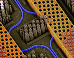
IBM’s foray into this arena involves using light instead of electrical signals to process data in future computational applications. Using sub-100nm technology, the company is working on chip designs that would allow the integration of different optical components side-by-side with electrical circuits on a single silicon chip using sub-100nm technology.
Light Pulses
IBM has created 90nm Silicon Integrated Nanophotonics technology, which interconnects silicon-nanophotonics circuits and silicon transistors. The design uses light pulses for communication purposes, and provides a very fast and broad highway to process large volumes of data. A decade in the making, IBM is convinced the technology is close to moving silicon nanophotonics into today’s chip manufacturing environments.
This looks like good timing for IBM. It’s a recognised fact that many business operations today rely heavily on computing and communications systems that can receive, analyse, and respond to vast data amounts. Subsequently, only those that can successfully handle such loads will survive what is often called the “Big Data” scenario: Processing requirements so large and complex that it becomes difficult to process using available database-management tools or traditional data-processing applications.
IBM says that its Silicon Nanophotonics technology will meet the Big Data challenges by connecting various parts of large systems, whether a few centimetres or kilometres apart from each other. On top of that, it will be able to move terabytes of data via pulses of light through optical fibres.
By adding processing modules into a 90nm CMOS fabrication line, IBM integrated various silicon-nanophotonics components, such as wavelength division multiplexers, modulators, and detectors, within CMOS electrical circuitry. This approach will undoubtedly keep the cost of nanophotonics down. The company has already created transceivers that can shift data at 25Gbps per channel.
In addition, the technology can feed a number of parallel optical data streams into a single fibre via multiplexing devices. The ability to multiplex large data streams at high data rates will allow for future scaling of optical communications that ultimately deliver terabytes of data between distant parts of computer systems.
About the Author
Paul Whytock
Comment About the Article
To join the conversation, and become an exclusive member of Electronic Design, create an account today!

Leaders relevant to this article: