The Active Clamp Flyback Converter: A Design Whose Time Has Come (.PDF Download)
One trend that shows no size of ending is the move to smaller personal electronic devices. From smartphones to tablets, each successive generation is smaller and more powerful than the last. It’s usually battery-powered and must be regularly charged by an external charger or adapter.
The movement to more powerful processors and larger screens poses a challenge for the power designer, who must continually come up with new ways to boost efficiency and reduce battery-charger size. Stringent new standards such as DoE Level VI and EU CoC V5 Tier-2 raise the efficiency requirements on a wide range of power adapters.
As a result, designers must improve the design of the discontinuous-mode quasi-resonant flyback topology. Such a converter is traditionally used to implement a low-cost ac-to-dc power adapter for power levels up to 100 W.
A flyback converter uses relatively few components, is simple to design, and can accommodate multiple outputs. With a silicon power MOSFET, its efficiency can run as high as 90% if synchronous rectification is employed and the switching frequency is kept below 100 kHz to reduce switching losses.
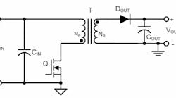
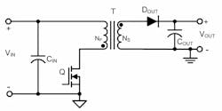
Figure 1 shows the essential elements of the flyback design. The transformer acts as a coupled inductor rather than as a true transformer. When the power switch is on, the flyback converter stores energy in the primary-side inductor. During the switch off time, the energy transfers to the secondary and from there to the output. Current flows in either the primary or secondary winding, but not both at the same time.

