Additions Boost Fault-Protected Current Limiter Precision At Higher Supply Voltages
A previous Idea for Design described a technique for protecting the “pass” transistor in a current-limiting circuit against excessive power dissipation (see “Fault-Protected Current Limiter Keeps Its Cool”). Although highly effective at low supply voltages, the technique lacks precision above 10 V. Also, changes in ambient temperature can cause variations in the trip point. Adding a few inexpensive components can significantly improve the circuit.
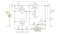
The conventional circuit uses transistors Q1 and Q2 to create a current limit, ICL, which is set by R1 (inside the dashed line in Figure 1):
ICL ≈ VBE(Q1)/R1
where VBE(Q1) is Q1’s base-emitter voltage, normally about 0.7 V.
1. A simple current-limiter circuit (inside the dashed line) is very effective at low supply voltages but lacks precision at supply voltages above 20 V. The additional components protect the circuit at higher voltages and against drops in load resistance.
This simple circuit is fine if ICL is relatively small and the supply voltage isn’t too large. But in the event of a fault caused by either an excessive increase in supply voltage or an abnormally low load resistance, the power dissipated in the pass transistor, Q2, can become too high.
For example, if the circuit is designed for ICL = 100 mA and a supply voltage, VS, of 20 V, a short circuit across the load could dissipate almost 2 W in Q2. A small-signal transistor like the 2N3906 can’t handle power levels above 625 mW, so a larger transistor with additional heatsinking would be needed to maintain a safe junction temperature. In many applications, the additional cost could be prohibitive.
Related Articles
• Regulator Limits Dissipation While Capping Current At The Desired Level
• Whitepaper: Average Current Limit Balances Center Point of Half-Bridge Input Caps
• Fault-Protected Current Limiter Keeps Its Cool
The additional components in Figure 1 eliminate this problem. Q3 and IC1 form a power-monitoring circuit that cuts off Q2 if its dissipation exceeds a predetermined level. The IC—an adjustable, precision, shunt voltage regulator—integrates a voltage reference, comparator, and open-collector output in a three-pin package.
The voltage at its Ref input, measured relative to its anode terminal, is compared to an internal voltage reference, VRef, nominally 2.5 V. In the “off” state, when the Ref input is 0, the current into the cathode terminal is less than 1 µA. As the Ref input approaches VRef, the cathode current increases slightly. When the Ref input exceeds the 2.5-V threshold, the device switches fully “on” and the cathode voltage (relative to the anode) falls to about 2 V.
IC1 and divider R5/R6 monitor Q2’s collector-emitter voltage, VCE(Q2). The values of R5 and R6 are chosen to make the voltage across R6 (that is, the Ref voltage) precisely 2.5 V when VCE(Q2) reaches a critical value. When that happens, IC1 turns on, pulling current through R4 and biasing Q3 fully on. In turn, this clamps Q2’s base-emitter voltage almost to 0, so Q2 turns off and the load current drops to 0.
The critical value of VCE(Q2) depends on its maximum power rating, PD(max) and ICL. For example, if Q2 is a 2N3906 with a maximum dissipation of 625 mW at 25°C, then PD(max) can be set at 500 mW to allow a safe margin. If ICL = 100 mA, the power in Q2 will reach 500 mW when its collector-emitter voltage is 5 V.
You can determine R5 and R6 by:

For example, if PD(max) = 500 mW, ICL = 100 mA, and VRef = 2.5 V, then R5 = R6.
Using these values and a VS of 20 V, the power in Q2 increases linearly as the load resistance is reduced below 180 Ω since the circuit is in its current-limiting region (Fig. 2). When the load drops to about 144 Ω, Q2’s power reaches 494 mW. Reducing the load below 144 Ω causes Q2’s collector-emitter voltage to reach 5 V, at which point IC1 and Q3 turn fully on and cut off Q2. The dissipation immediately falls to 0, preventing damage to Q2.
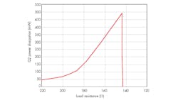
2. Results from the example circuit show its very fast response, dropping Q2’s power dissipation to 0 if the load resistance drops to a dangerous level.
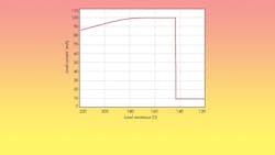
The load current changes correspondingly as the load resistance is reduced. Initially, the current ramps up linearly until it levels off at about 100 mA, the current-limiting region (Fig. 3). At the point where Q2 cuts off, the load current immediately falls to about 10 mA. The circuit is now latched in its “tripped” state, where the relatively low load current consists almost entirely of the current though IC1. The circuit remains in this off state until either the supply voltage is cycled off-on or until the load is disconnected.
3. The circuit’s load-current response to reducing the load resistance illustrates the current-limiting region from about 180 Ω to about 144 Ω, where the circuit trips, reducing current to 10 mA.
The circuit ensures fast, precise protection for the pass transistor, Q2. Because the circuit is so sensitive, C1 may be required to filter noise from IC1’s Ref input to prevent nuisance tripping. Also, because the circuit responds so quickly, loads such as motors or capacitive loads that create a large in-rush current may cause false tripping.
Anthony M. Smith has been working as a consultant engineer for the past decade, designing products for the industrial, domestic, and automotive markets. He received a BSc (Honors) in electronics from Salford University, Greater Manchester. He also holds two patents. He can be reached at tony@ [email protected].
About the Author
Anthony Smith
Consultant Engineer
Anthony M. Smith has been working as a consultant engineer for the past decade, designing products for the industrial, domestic, and automotive markets. He received a BSc (Honors) in electronics from Salford University, Greater Manchester. He also holds two patents.
Comment About the Article
To join the conversation, and become an exclusive member of Electronic Design, create an account today!

Leaders relevant to this article: