Relays usually are driven using optocouplers, which offer isolation between analog and digital grounds to ensure that switching currents in the relay coils do not affect the noise margin of the digital circuit. For driving a large number of relays through a bus-based backplane, the on-board complex programmable logic device (CPLD)/FPGA provides the interfacing and diagnostics to the I/O board.
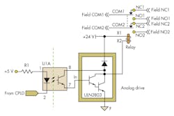
A ULN2803 Darlington transistor with base current controlled by the optocoupler drives the relay. To minimize power for CPLDs, their outputs are connected to the cathode of the optocoupler, while the anode is connected to either +5 V through a current-limiting resistor.
In a typical backplane bus-based system, +5 V and +24 V are used for powering the digital logic and relay coil, respectively. The problem begins when we independently switch off the digital-circuitry power supply before the relay-coil supply. In the circuit of Figure 1, the CPLD has to output a logic “1” (+5 V) to ensure that the relay is switched off. When the digital power supply is switched off, the power supply begins to decay, with the time constant depending on the load.
As +5 V reaches 2.5 V, the CPLD output goes to logic zero, causing the optocoupler to switch the Darlington transistor ON. This, in turn, energizes the relay. As the power supply decays to +1.2 V, it turns the optocoupler off, which in turn de-energizes the relay. This intermittent energizing of relays can cause problems in critical applications due to improper power sequencing.
For example, the relay may be driving a safety valve and a power switch-off would cause the safety valve to actuate or de-actuate, resulting in a critical process disturbance. A similar event takes place during power-on, when +5 V ramps up slower than +24 V.
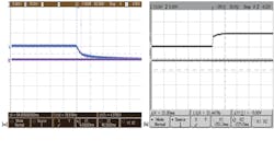
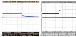
The blue and pink lines in Figure 2 represent the +5 V and relay’s normally open (NO) contact, respectively. The duration of the energization is directly related to the time between the +2.5-V to +1.2-V transition, after which the relay gets permanently de-energized.
Solutions: First Strategy
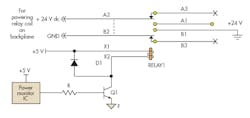
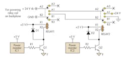
This undesirable situation must be avoided at all costs, particularly when the relays are driving safety systems. The suggestions for a design change for the existing system in a plant would have severe financial implications. The simplest way to mitigate this problem is to ensure proper power sequencing during power-on and power-off conditions (Fig. 3).
The tactic is to supply interrogation voltage to the relay coil through the intermediate logic (piggyback board) rather than directly from the +24-V power supply. The circuit consists of a power-monitor IC, a transistor, and an external relay. During the normal operation, when the +5 V is stable, transistor Q1 is on, the relay is energized, and +24 V is supplied through the contacts of the external relay.
The power-monitor IC continuously monitors the power line. During the power-off transient, when the voltage goes below 4.63 V, the transistor switches off. This in turn de-energizes the relay, which then rapidly cuts off the power supplied to the relay coil.
Related Articles
- Driver Saves Power In Energized Relay
- Simple Circuit Reduces Relay Coil Power
- What's All This Solenoid Driver Stuff, Anyhow?
Since the +24-V supply is removed instantaneously, the relays do not experience any intermittent switching. Similarly, during the power-on condition, the power-monitor IC generates an active-high output 200 ms after +5 V reaches stability. This, in turn, switches on the transistor and the following relay, with the relay coil supply to the slave I/O boards restored.
So during power-on and power-off transient, this circuit minimizes intermittent relay energization of I/O boards. The only design consideration is the choice of the external-relay contact rating, which must be chosen for the maximum load. .
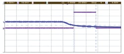
The circuit addresses the stuck-high failure for the power-monitor IC or short-circuit-mode transistor failure. The stuck-low failure for the power-monitor IC and open-mode failure of the transistor will lead to spurious trip, which is safe and can be tolerated in many critical systems (Fig. 4). Figure 5 shows the associated waveforms for power on and power off, respectively.
Solutions: Second Strategy
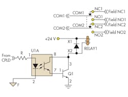
The classical relay-driver design with the CPLD/FPGA driving the optocoupler in sinking mode is the main cause of the problem. The sourcing mode could be chosen at the expense of dissipating more power from the CPLD (Fig. 6). One solution is to use a Darlington transistor (Q1) to drive the relay. But during the de-energization phase, the relay contacts are held for a finite amount of time, due to the high β of the transistor. This circuit also eliminates intermittent relay.
Solutions: Third Strategy
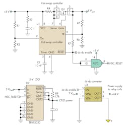
For those designs that are power sensitive and where the sinking mode of operation cannot be avoided, the use of a hot-swap controller (HSC) along with a dc-dc converter can solve the problem (Fig. 7).
The HSC reset output directly controls the enable/disable function of the +5-V to +24-V dc-dc converter. The HSC then initiates an active-low reset signal whenever the +5-V power is less than +4.63 V, and this signal disables the dc-dc converter. When +5 V is stabilized, the dc-dc converter is enabled.
Similarly the dc-dc converter is switched off in less than a few microseconds during the +5-V switch-off condition. The HSC has added features such as short-circuit protection, overload, and under-voltage lockout, coupled with power-sequencing logic. This method requires additional ICs and a dc-dc converter, which eats up the real estate and component count.
Conclusion
Each of the three strategies and methods for the relay driver design has certain merits and demerits. The first strategy provides a system-level solution, whereas the second and third strategies provide board-level solutions. Hence, the tradeoff must be carefully analyzed and the design strategy must be appropriately chosen to fit the purpose.
G.V. Kishore, N. Sridhar, and K. Palanisami are with the Electronics & Instrumentation Division of the Indira Gandhi Center for Atomic Research, Kalpakkam, Tamilnadu, India.
