For low-power devices powered by alkaline or lithium primary batteries, every microampere of current becomes critical for extending battery life and increasing the time between battery replacements. This is especially true when the primary device being powered is a low-power microcontroller (MCU)—significant power savings can be achieved by exploiting the typically wide input-voltage range during the microcontroller’s sleep or standby modes.
This file type includes high resolution graphics and schematics when applicable.
When using a boost converter between the battery voltage and microcontroller, switching it off and simply passing the input voltage to the output dramatically improves system efficiency. Basically, the boost converter’s operating current is replaced with its much lower shutdown current. This article presents such a concept for a metering application, and compares the battery-life improvement from a boost-plus-bypass converter versus other methods of powering the MCU.
Powering an MCU Directly from the Battery
A low-power optimized MCU typically supports a wide supply voltage range, such as 1.8 to 3.6 V.1 As a result, the MCU’s embedded system can incorporate a flexible power architecture. Subsequently, it’s possible to combine the MCU’s power supply with another existing power supply in the system, 2.5 V for example, to simplify the system power architecture. In this way, only one power supply is required for the system, which reduces cost.
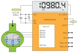
The MCU’s wide input voltage range also supports being directly powered from batteries, which have varying voltages based on their state of charge. For example, a CR2032 coin cell’s voltage typically ranges from 2 to 3 V, while two AA alkaline batteries connected in series produces a voltage of around 1.8 to 3.3 V. Both of these battery’s voltages line up perfectly with an MCU, which requires between 1.8 and 3.6 V to function. For some very low-cost systems, the best approach is a direct connection of the batteries to the MCU and system with no power supply in between. Figure 1 shows this arrangement using a coin cell as the MCU’s power source.
For other systems that contain multiple subsystems running off of the same voltage rail, this direct connection may not fully utilize all of the battery’s energy. For example, in a metering application with a MCU, sensor, and motor, the motor might require at least 2.2 V to function. If the battery connects directly to the system, the system can’t operate below the motor’s 2.2-V cutoff voltage. Thus, some energy remains in the battery that’s not extracted. This shortens the system’s operating time from what it would be if all of the battery’s energy was used.
Powering an MCU with a Boost Converter
Utilizing the remainder of the battery’s energy in systems with a higher cutoff voltage requires a boost converter between the battery and the system. The boost converter is only needed when the battery nears depletion, which means less than 2.2 V in this example. If the boost converter is active at other times, it unnecessarily boosts the battery voltage to the system.
Since the system doesn’t need the higher voltage with higher battery voltages, having an always active boost converter simply wastes battery power due to the converter’s current consumption. This current might be as high as 10 µA, whereas the MCU and system may consume only 700 nA in standby.1 Though the boost converter allows operation to drop to lower battery voltages, the extra power consumed is quite significant for systems with lengthy standby times.
Powering an MCU with a Boost-Plus-Bypass Converter
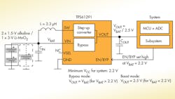
Ideally, these systems need a boost converter when the battery is near its end of discharge and too low to supply the system, but a direct connection between the battery and system otherwise. This is known as a boost-plus-bypass function. A boost-plus-bypass converter is a boost converter that also includes a switch directly from its input to its output (Fig. 2). This is controlled by the MCU to either boost or bypass the battery voltage. Such a combination enables the direct connection for higher battery voltages in addition to a boost function that extracts the battery’s last remaining energy.
Performance Comparison
Figure 3 compares the battery current drawn from three systems—direct battery connection, boost converter, and boost-plus-bypass converter—using an MCU and subsystem that draws 700 nA in standby operation. Because the boost-converter topology must increase the input voltage, the output voltage is set to 3.3 V. The boost-plus-bypass converter outputs 2.5 V only when the battery drops below 2.2 V. To achieve a fair comparison, the boost converter used is the same device as the boost-plus-bypass converter, but it doesn’t operate in bypass mode. The quiescent current (IQ) of the boost-plus-bypass converter in boost operation is the same 5.7 µA drawn from its output.2,3
The boost-plus-bypass converter requires a mere 15 nA to operate in bypass mode; therefore, it draws slightly more current than the direct connection. Unlike most traditional boost converters, which set the output voltage with an external resistor divider, the boost-plus-bypass converter shown has an internal resistor divider. It’s disconnected in bypass mode so that it doesn’t draw any current.
Whereas the direct-connected system stops working at 2.2 V, the boost-plus-bypass system keeps operating down to 2 V and even lower, if supported by the battery’s chemistry. The boost-converter system draws significantly more current on a logarithmic scale for the entire battery voltage range. An additional advantage of the MCU-controlled boost-plus-bypass converter is the ability to boost the battery voltage at any time, such as for programming the MCU.
Conclusion
A boost-plus-bypass converter extends the battery run time in embedded MCU systems, which operate in standby mode for long periods of time. The extremely low current consumption in bypass mode doesn’t excessively drain the battery, while enabling the batteries to operate at lower voltages significantly extends battery life in metering and other applications.
This file type includes high resolution graphics and schematics when applicable.
Christopher James Glaser, applications engineer for TI’s Low Power DC/DC group, supports customers, designs evaluation modules (EVMs), writes application notes, trains field engineers and customers, and generates technical collateral to make TI parts easier to use. He received his BSEE from Texas A&M, College Station, Texas. He can be reached at [email protected].
References:
- MSP430FW427 ultra-low power MCU
- IQ: What it is, what it isn’t, and how to use it, Chris Glaser, Analog Applications Journal (SLYT412), Texas instruments, 2Q 2013
- TPS61291 datasheet
About the Author
Chris Glaser
Applications Engineer
Christopher James Glaser is an applications engineer for TI’s Low Power DC/DC group. In this role, he supports customers, designs evaluation modules (EVMs), writes application notes, trains field engineers and customers, and generates technical collateral to make TI parts easier to use. He received his BSEE from Texas A&M, College Station, Texas. He can be reached at [email protected].
Voice Your Opinion!
To join the conversation, and become an exclusive member of Electronic Design, create an account today!

Leaders relevant to this article:


