GaN Devices Power the Next Generation of LiDAR Systems
This article is part of the TechXchange: LIDAR Technology
Download this article in PDF format.
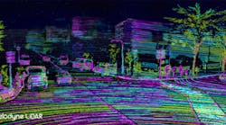
The goal of a sensor is to gather data about a real-world parameter and convert it to electrical form. Needless to say, the techniques for doing that take many forms, but the standard method to determine distance measures the time taken for a transmitted signal to travel to a target object and be reflected back to an adjacent receiver. The signal can be acoustic, as in a sonar or ultrasonic system, or electromagnetic (EM) waves, i.e., radar (radio direction and ranging) and LiDAR (light detection and ranging) (Fig. 1).
Sponsored Resources:
- Break the Speed Barrier with GaN Drivers
- GaN drivers - switching faster than today's technology
- Nanosecond Laser Driver Reference Design for LIDAR
1. The latest automotive LiDAR systems provide a detailed image of a vehicle’s surroundings (Source: Velodyne)
Both radar and LiDAR systems transmit and receive EM waves. As its name suggests, a radar system uses radio-band frequencies up to several hundred gigahertz (Fig. 2). LiDAR, though, operates at much higher frequencies: the portion of the spectrum from near-infrared (IR) to visible blue light. Because LiDAR’s higher frequencies in turn provide higher resolution, it’s widely used for topographical mapping, adaptive cruise control, and emergency braking. Furthermore, it’s expected to play a key role in collision-avoidance systems in autonomous vehicles.
2. LiDAR and radar operate on similar principles, but use radically different wavelengths. (Source: radartutorial.eu)
Figure 3 shows the block diagram of a LiDAR system for simple distance measurements using the time-of-flight (ToF) method. Light emitted by the laser is first focused by a lens to create a narrow beam, which then travels to the target, is reflected, returns, and is focused on the detector by a second lens. The laser driver and stimulus subsystem can be designed to apply pulsed or amplitude-modulation (AM) waveforms.
3. Shown is a simplified block diagram of a LiDAR system for ToF distance measurement. (Source: TIDA-01187: “LIDAR-Pulsed Time-of-Flight Reference Design Using High-Speed Data Converters” PDF)
The optical detector is typically a PIN or avalanche photodiode, which produces a small current proportional to the return signal. The amplified return signal is measured and processed to produce a range measurement.
A scanning LiDAR system goes beyond ToF to produce a high-resolution 3D map of the environment. An automotive LiDAR system, for example, scans the vehicle surroundings horizontally to produce a composite 360-degree image.
In most current implementations, a moving mirror deflects the laser beams. Several laser diodes can be stacked to extend the vertical field of view. A mechanical mirror is bulky, expensive, and unreliable, though. Manufacturers are now developing specialized integrated circuits that combine multiple laser diodes and microelectromechanical-system (MEMS) deflection technology.
At a theoretical level, the maximum range Rmax of a LiDAR system is given by the LiDAR equation:
where Ps = transmitted power; G = antenna gain at the chosen wavelength; λ = wavelength; PEmin = minimum detectable power; and σ = effective target cross-section.
The effective target cross-section σ depends on such factors as the target reflectance at the laser wavelength, the scattering solid angle (steradians), and the target area.
These equations contain many variables and constants, and reliable estimates are difficult to determine for a given set of conditions. In practice, designers make simplifying assumptions about variables and use empirically determined values for constants.
Practical Design Requirements for LiDAR Systems
An autonomous vehicle must be able to discriminate between other vehicles, buildings, road signs, pedestrians in dark clothing, etc., all while traveling at high speeds. Not surprisingly, then, the performance requirements for a LiDAR system are continually increasing, especially for resolution and effective range. For high-speed applications, the system must be able to detect an object with 10% reflectivity at a distance of 300 m and distinguish between objects 30 cm in size.
This specification translates into a design that requires 100 to 200 W of optical power and a repetition rate of up to 1 MHz to fill a front-facing field of vision (100° × 25° with a 0.1° resolution) and allow for a 20- to 60-Hz refresh rate.
But there’s a catch: Lasers transmitting in the near-IR and visible regions can cause eye damage, including retinal burns, corneal burns, and cataracts. The IEC60825-1 safety specification classifies a laser based on the maximum permissible exposure (MPE) limit of the human eye. The MPE is defined as the highest power or energy density (in W/cm2 or J/cm2) of a light source that’s considered safe.
Because it’s used in an uncontrolled environment—no safety goggles for passers-by or other drivers—a LiDAR laser must be rated as Class 1: Safe under all normal operating conditions. Operating at the popular near-IR wavelength of 905 nm, the laser must be within the eye safety energy limit of 250 nJ for continuous exposure.
From the equation above, increased range requires more power. And increased resolution needs a higher sample rate. The only way to meet both the safety limits and the performance requirements is to have an extremely high energy pulse for an extremely short amount of time and transmit it at an extremely low duty cycle.
The refined requirement then becomes 100 to 200 W transmitted as a pulse of 1 to 2 ns at a 1- to 2-MHz repetition rate.
GaN to the Rescue
With an optical power requirement of up to 200 W and a laser-diode efficiency of around 50%, the driver circuitry must provide a 1- or 2-ns current pulse of 30 to 60 A. To achieve this, designers are increasingly turning to gallium-nitride (GaN) technology. GaN is a wide-bandgap semiconductor that’s becoming the preferred solution for many high-power, high-speed switching applications.
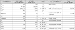
4. A GaN HEMT has lower conduction and switching losses than a Si MOSFET, giving it superior performance in high-speed power-switching applications. (Source: TI Designs—Power Management: Nanosecond Laser Driver Reference Design for LiDAR)
The GaN high electron mobility transistor (HEMT) provides superior performance to a traditional silicon FET in the LiDAR system. Figure 4 compares the specifications of a 60-V silicon power transistor and an equivalent GaN device with the key differences noted. The RDS(on) of the GaN part is around half that of the silicon device; its conduction losses are reduced by 50%, leading to a smaller package and shrinking the size of any cooling components.
The advantage of the GaN device is most clearly illustrated when comparing switching loss. Its transconductance (gm) is almost five times higher, so it has only 20% of the switching loss of the silicon part.
The GaN device does have one disadvantage—it requires twice as much charge for the output capacitance COSS, resulting in twice the losses. But overall, when switching 30 A, the GaN part shows a power savings of 2 W.
LMG1020 GaN Driver: A Key Piece of the Puzzle
An FPGA, ASIC, or microcontroller (MCU) controls the timing of the GaN pulse, but these devices aren’t designed to drive the GaN transistor directly. One reason is that the PWM signal from the digital device is often a 3.3-V logic signal, which must be level-shifted to fully turn on a power switch that requires 5-V VGS. The switch may still turn on with a 3.3-V VGS, but the conduction losses will be much higher. At megahertz switching speeds, the digital output pin also can’t supply the high dynamic current requirements of the power device, slowing the turn-on and turn-off times and increasing switching losses.
A gate driver provides the buffer-drive function between the PWM output of the controller and the gate of the GaN transistor. Locating the high-current driver close to the power switch also minimizes the effect of high-frequency switching noise on other devices, as well as reduces the controller’s power dissipation and thermal stress.
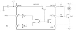
5. The LMG2010 buffers the PWM signal from an MCU or FPGA, and provides the voltage and current needed to drive the GaN power FET. (Source: TIDA-01573: Nanosecond Laser Driver Reference Design for LiDAR)
The LMG1020 (Fig. 5) is a single low-side driver targeted at GaN HEMTs and logic-level silicon FETs in high-speed applications. The simple structure of the device allows for extremely fast propagation delays of 2.5 ns for signals as short as 1 ns. The drive outputs for the pullup and pulldown edges can be independently adjusted via external resistors up to maximum values of 7 A (source) and 5 A (sink), respectively. The part features undervoltage lockout (UVLO) and overtemperature protection (OTP) to ensure it’s not damaged in overload or fault conditions.
At these high power levels and fast switching speeds, it’s important to minimize the parasitic inductances, particularly in the laser power loop that carries the highest current. These inductances can cause overshoot and impose excessive stress on other components.
The LMG1020 comes in an extremely compact, low-inductance 2×3 ball WCSP chip-scale package, but the PCB layout and selection of the other components also play a key role. Reference design TIDA-01573 includes an in-depth discussion of component selection and layout best practices when the LMG1020 is used to drive a LiDAR laser diode. These include:
- Separation of the power loop ground and gate loop grounds
- Addition of micro-vias in pads to reduce the parasitic inductances
- Minimization of return loops
- Selection, placement, and values of bypass capacitances
- Power-supply considerations
- Clamping diode selection
Incidentally, GaN isn’t used only in LiDAR—it’s also playing a key role in other power systems. TI's LMG1210, for example, is a GaN driver with adjustable dead time that’s optimized for ultra-compact half-bridge applications. These include class-D audio amplifiers, motor drives, and envelope tracking for emerging 5G mobile applications.
You can find out more about TI’s GaN products on the Solutions Overview page.
TDC7201 Simplifies LiDAR Receiver Design
To complete the LiDAR design, the received pulse must be captured and compared with the transmitted pulse to determine the range. A scanning system requires complex digital processing to build up a complete environmental map, but specialized devices are available to simplify ToF applications.
The TDC7201 (Fig. 6) is one such device. It contains two built-in time-to-digital converters (TDCs) and can measure distances from 4 cm to several kilometers without requiring external FPGAs or processors.
6. The TDC7201 simplifies the receiver portion of a LiDAR ToF design. (Source: “TDC7201 Time-to-Digital Converter for Time-of-Flight Applications”)
Each TDC acts as a stopwatch and measures the elapsed time between a START pulse and up to five STOP pulses. The ability to measure simultaneously and individually on two pairs of START and STOP pins with two built-in TDCs provides high design flexibility.
The TDC7201 has an internal self-calibrated time base that compensates for drift over time and temperature. It also enables time-to-digital conversion accuracy in the picosecond range.
In addition, an Autonomous Multi-Cycle Averaging Mode optimizes operation for low-power applications. In this mode, the host MCU initiates the measurement sequence and switches to a low-power sleep mode. The TDC7201 wakes the MCU with an interrupt when it has completed the measurement.
A TDC7201 evaluation module is available.
Conclusion
A LiDAR system requires fast switching of high-current pulses to meet ever-increasing performance specifications. A GaN power switch can satisfy these requirements, but designers must choose the correct driver and follow good layout guidelines to be successful. Texas Instruments offers a range of components to meet both LiDAR and GaN power requirements.
Check out more content from the TechXchange: LIDAR Technology
Sponsored Resources:


