Improved Power ICs Give Supply Designers More Bang for The Buck

This file type includes high resolution graphics and schematics.
As the use of electronics in all sectors of society grows, so does the need for more efficient, higher-level, and more cost-effective power sources. This in turn is spearheading the development of power discrete devices like diodes, MOSFETs, integrated-gate bipolar transistors (IGBTs), gate turn-off and integrated gate turn-off (GTO and IGTO) thyristors, and power modules. Gallium-nitride (GaN) and silicon-carbide (SiC) power devices also await.
Power-supply designers now can choose from a wide variety of power devices that pay handsome dividends for their designs. According to IMS Research’s Power Semiconductors Discretes and Modules report, the total market value of these devices grew last year by 3.7% to $13.5 billion and continues to grow rapidly. MOSFETs and IGBTs will lead the growth, though IGBTs are expected to grow at a faster rate.
MOSFETs Vs. IGBTs
MOSFETs and IGBTs are similar yet offer different performance levels. An IGBT combines the simple gate-drive characteristics of a MOSFET with the high-current and low-saturation voltage capability of a bipolar transistor. An IGBT combines an isolated gate FET for the control input with the bipolar transistor acting as a switch (Fig. 1).
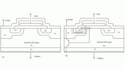
1. An IGBT combines the simple drive characteristics of a MOSFET with the high-current and low-saturation-voltage capabilities of a bipolar transistor. It achieves this by combining an isolated-gate FET for the control input with the capability of a bipolar transistor as a switch in a single structure (a). Its construction is similar to that of an N-channel MOSFET except the N+ drain is replaced with a P+ collector layer to form a vertical pnp bipolar junction transistor (b). (courtesy of Wikipedia.org)
IGBTs are used in medium-power to high-power applications such as switched-mode power supplies (SMPSs), traction motor control, and induction heating. Typically, large modules include a number of IGBTs in parallel and feature current-handling capabilities of hundreds of amperes with blocking potentials of 6000 V and kilowatts of power handling capability.
One example, the 1.2-kV, 60-A MIXA60WH1200TEH converter-brake-inverter module from IXYS Corp., comes in an E-3 pack that’s just 1.7 mm high. It combines bipolar power with what IXYS calls eXtremely rugged, eXtremely light Punch Through (XLP) IGBTs. It is designed for energy-efficient power supplies, uninterruptable power supplies (UPSs), motor control, and inverter applications.
There is a gray area where either MOSFETs or IGBTs can be used for applications involving blocking voltages of about 250 V to 1 kV and switching frequencies somewhere between 25 kHz and 250 kHz. Here, the chosen device is very application-specific, cost, size, switching speeds, and thermal cooling requirements come into play.
There also are some drawbacks to IGBTs. Because of their on-state voltages, they feature a lower switching speed, especially at turn-off time. This is because during the turn-off period electron flow can be stopped rather abruptly, just as it can be stopped for a power MOSFET, by reducing the gate-emitter voltage below the threshold voltage.
In the case of an IGBT, holes are left in the drift region in IGBTs. This leads IGBTs to exhibit a tail current during turn-off time until all the holes are swept out or recombined.
Some IGBTs known as non-punch-through (NPT) devices incorporate an n+ buffer layer that quickly absorbs trapped holes. Those that don’t are called punch-through (PT) IGBTs.
On-state latch-ups are another potential IGBT downside. They can be problematic for an IGBT when it is operated outside its data-sheet ratings and result in a failure mode where the IGBT no longer can be turned off by the gate.
IGBTs continue to improve their already low switching losses. The 650-V TrenchStop 5 process from Infineon Technologies reduces switching losses by more than 60% compared to current leading solutions. Its thin wafers provide what Infineon calls best-in-class IGBT performance. The 650-V devices produced on the process are available in TO-220, TO-220 FullPak, and T0-227 packages (Fig. 2).
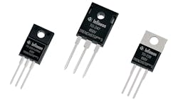
2. The Infineon Technologies 650-V TrenchStop 5 process reduces switching losses by more than 60% compared to current leading solutions. Thin wafers provide what Infineon calls best-in-class IGBT device performance. The devices are available in TO-220, TO-220 FullPak, and T0-227 packages.
Fairchild Semiconductor’s FGAxxSxxP shorted-anode 1.1-kV to 1.4-kV IGBTs target high-power and high-frequency applications like induction heating. Compared to typical NPT IGBTs, they offer a 12% lower saturation voltage and a 20% lower tail current. They also are optimized with intrinsic anti-parallel diodes for soft switching applications.
IGBTs are used in many industrial, transportation (railroads, heavy offroad equipment), automotive, military/aerospace, commercial, and geothermal applications. They offer reduced conduction losses and greater efficiency at higher currents than MOSFETs, according to International Rectifier, which makes both IGBTs and MOSFETs. IR’s COOLi2R platform features silicon and packaging technology advances for hybrid and electric-vehicles to help reduce the size, weight, and system costs of electric power train components while increasing reliability (Fig. 3).
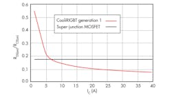
3. IGBTs like those made on International Rectifier’s CoolIR2 platform offer reduced conduction losses and greater efficiency at higher currents than MOSFETs. (courtesy of “IGBTs or MOSFETs: Choose Wisely” by Carl Blake and Chris Bull, International Rectifier.
MOSFETs also are used in SMPSs and operate at frequencies in the hundreds of kilohertz. But unlike IGBTs, MOSFETs have no theoretical on-state resistance (RDS(on))limits. IR’s IRPF4137P13F MOSFETs deliver benchmark RDS(on) performanceof 69 mΩ and a total gate charge (Qg) of 8.3 nC in TO-220 and TO-247 packages. The 70-A IRPF4868PF has an RDS(on) of just 32 mΩ and a Qg of 180 nC in a TO-247 package.
Because a MOSFET has a body-drain diode, it is particularly useful in dealing with limited free-wheeling currents. But MOSFETs have generally been limited to blocking voltages of 250 to 300 V and can be found mostly in computer and consumer electronics products and digital logic circuits.
This lower voltage-blocking capability is beginning to change thanks to the development of super-junction MOSFETs from many power semiconductor IC manufacturers that have allowed them to produce MOSFETs with 400-V+ voltage-blocking capabilities. These newer super-junction MOSEFTs can be manufactured on smaller die sizes, making them less expensive to produce, and feature low on-state resistance levels. They’re now being considered for hybrid and electric vehicle low-end designs. Marketing analyst Yole Développment foresees super-junction MOSFETs that can handle l kV by 2018.
The main difference between the present crop of super-junction MOSFETs and IGBTs is that the former has higher on-state losses at high current levels than the latter. Super-junction MOSFETs are simpler to manufacture and, thus, less expensive. IGBTs operate at higher temperatures than super-junction MOSFETs, but those MOSFETs are improving and catching up to the IGBT’s maximum operating temperature.
Infineon Technologies makes available 400-V+ super-junction MOSEFTs using its CoolMOS power platform. Producing them involves using multiple epitaxial layers and doping steps to create a locally doped island in the epitaxial layer. The doped region then diffuses and creates an N-doped pillar.
Other companies like Toshiba, Fairchild Semiconductor, and IceMOS Technology use reactive ion etching. This allows them to dig a trench that’s filled with an N-doped material to create the super-junction MOSFET.
Toshiba’s TK100S04N1L MOSFET suits high-speed automotive switching. It achieves a low on resistance of just 1.9 mΩ (at a VGS of 10 V) and a low leakage current (IDSS) of 10 µA maximum in a DPAK package. Toshiba credits its eighth-generation trench MOSFET technology and the use of low-on-resistance copper interconnects. The device is rated to operate at up to 175°C.
STMicroelectronics offers the Power Trench program. Its SuperMesh5 platform enables the development of 900-V (STx1N9DK5) and 850-V (STx20N95K5) MOSFETs for driving LEDs. They’re aimed at eco-friendly designs and are available in IPAK packages. An 850-V variant, the STx23N85K5, is available in a PowerFlat 1-mm-thick surface-mount technology (SMT) package (Fig. 4).
4. STMicroelectronics’ SuperMesh5 900-V and 850-V MOSFETs are designed to drive LEDs in eco-friendly designs. They’re available in IPAK packages. An 850-V variant is available in a PowerFlat 1-mm thick package.
Fairchild Semiconductor offers the FSL1x series of high-voltage FPS Green Mode Power Switches. These 650-V, 700-V, and 800-V devices are manufactured on the company’s vertical DMOS platform and provide high efficiency levels for SMPSs.
A milestone in the development of highly integrated MOSEFT power devices is the EN2300 from Enpirion Corp. The 4-A to 15-A buck converter module includes a controller, inductor, filter capacitors, and MOSFETs, all in a single quad flat no-lead (QFN) package (Fig. 5).
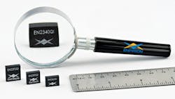
5. Enpirion’s EN2300 4- to 15-A buck converter module includes a controller, inductor, filter capacitors, and MOSFETs, all in a single QFN package.
Trench technology also is being used to make IGBTs. ON Semiconductor has expanded its portfolio of IGBTs made on its Trench Field Stop power platform to address hard-switching and soft-switching applications like motor inverter and induction heaters.
The devices are rated at 1.2 kV and can handle 15, 25, and 40 A. They feature switching frequency ranges of 2 to 20 kHz, 15 to 30 kHz, and 10 to 40 kHz, as well as low switching losses, a low Qg, and a wide operating temperature range of –55°C to 150°C.
High efficiency and ruggedness are two of the characteristics of IGBTs as shown by IR’s 1.2-kV IRGBCHxxxK10F family with best in class performance for industrial and energy-saving applications. Built on the company’s Gen8 Trench Gate Field Stop platform, whose design allows record-setting low VCE(ON) performance of 1.7 V, the thin wafer technology delivers improved thermal resistance and a maximum junction temperature of up to 175°C.
Here Comes GaN
For theoretical and practical reasons, silicon cannot sustain the higher-voltage and current capabilities needed for future hybrid and electric automotive, industrial, rail-transportation, photovoltaic inverter, and high-temperature radiation-hardened military/aerospace systems. Wide-bandgap compound semiconductors like GaN and SiC can significantly outperform traditional silicon.
Developments abound in trying to make GaN and SiC more practical and cost-effective to mass produce. Although they’re considerably more expensive, they’re beginning to make a bid as legitimate devices to power such things as LEDs. Yole Développment says that the market for GaN grew to nearly $10 million in 2012 and will grow to $500 million by 2016, up from $2.5 million in 2010.
GaN technology eliminates the need for packaging, slashing costs and wasted printed-circuit board (PCB) space, since it can be grown directly on a silicon substrate. The active GaN device can be isolated from the silicon substrate and completely encapsulated prior to singulation. And because it can be packaged in a flip-chip arrangement, thermal and electrical resistances are minimized.
Bulk GaN can be epitaxially grown on a CMOS process that it isn’t is compatible with, so relative newcomers to the power IC scene don’t need to establish CMOS processes in-house. Instead, they can rely on CMOS foundries that can work with them. Device makers then will be able to easily accommodate future demands quickly and at a potentially lower cost as CMOS wafer sizes grow larger from the present 2-in. and 4-in. wafers being used.
In fact, that’s exactly what’s happening. Some GaN device manufacturers that have shown that such devices can be manufactured are working closely with semiconductor fabrication houses. For example, GaN devices are already showing up as drivers for LEDs.
Toshiba is supplying mass-produced white light LEDs that use GaN chips manufactured on 200-mm silicon wafers. Together with Bridgelux Inc., Toshiba developed the process at a new production line at its Kaga Electronics Corp. in northern Japan.
Two ongoing process developments include growing bulk GaN on hybride vapor phase epitaxy (HVPE) GaN wafers. Another is growing bulk GaN on 2-in. and 4-in. ammonothermal GaN wafers. Both look promising in cost competitiveness with the growing of bulk GaN on larger 6-in. silicon wafers, when the much larger performance gains are factored in for using GaN wafers.
Efficient Power Conversion has already demonstrated that the production of GaN devices is possible using its 600-V eGaN devices. Using its EPC9102 demonstration board, EPC showed that its eGaN FETs can be used to make an eighth-brick (58 by 23 mm) fully regulated dc-dc converter that’s more efficient than silicon and that the output power can be increased by 33% at a 50% higher switching frequency using just 100-V eGaN devices.
International Rectifier is already supplying its IP2010 and IP2011 Integrated Power Stage GaN modules. According to the company, these modules allow SMPS designers to build switching converters at five to 10 times the switching frequencies presently used while maintaining the same efficiency.
The question now is when we can expect bulk GaN to become competitive with silicon. Lux Research analyst Pallavi Madakasira points out that the future of bulk GaN is going to come down to how it faces off against silicon substrates in his report, “Price or Performance:Bulk GaNVies with Silicon for Value in LEDs.”
Madakasirabelieves that by 2020, GaN grown on 2-in. wafers of HVPE can become competitive with bulk GaN grown on 6-in. silicon wafers, given the 360% performance improvements GaN on HVPE wafers offers over silicon (Fig. 6).

6. GaN grown on 2-in. wafers of HVPE can become competitive by 2020 with bulk GaN grown on 6-in. silicon wafers, given the 360% performance improvements that GaN on HVPE wafers offer over silicon. (courtesy of Lux Research).
The report also explores emerging new emerging materials such as aluminum nitride (AlN). It can be ideally suited for very low-wavelength ultraviolet LEDs, green laser diodes, and high-switching-frequency power electronics, and it may be an effective alternative to bulk GaN.
As with all emerging technologies, device modeling and characterization development tools are quickly emerging to validate the technology. A new version of the Agilent Technologies Integrated Circuit and Analysis Platform (IC-CAP) device modeling software for high-frequency characterization and modeling includes Angelov-GaN modeling and Python scripting.
SiC Coming Down The Road
Although not cost-competitive with silicon, SiC R&D efforts are accelerating in the development and manufacture of SiC power devices. Companies like Microsemi Corp. are offering samples of SiC power modules for high-temperature industrial applications. The APTxxxx family of modules boasts 1.2-kV and 600-V ratings that can handle 20 to 200 A in boost charger, phase-leg, and neutral-point clamped configurations.
Cree has shown that SiC can form the basis for impressive performance levels in LED lighting. Last year, the company used its S3 technology to demonstrate a prototype LED light bulb that produces 170 lumens/W, topping the 152-lumen/W level it previously announced. The S3 technology platform is designed to enable significantly higher-efficiency and lower-cost LED light bulbs for use in luminaires.
For now, designers of power electronics systems can be assured of a wide variety of IGBT and MOSFET devices to choose from. The GaN era is on the horizon but could take a few more years to become widespread commercial reality. And for those in need of maximum performance levels that other technologies can’t touch, SiC can deliver the goods.
This file type includes high resolution graphics and schematics.
About the Author
Roger Allan
Roger Allan is an electronics journalism veteran, and served as Electronic Design's Executive Editor for 15 of those years. He has covered just about every technology beat from semiconductors, components, packaging and power devices, to communications, test and measurement, automotive electronics, robotics, medical electronics, military electronics, robotics, and industrial electronics. His specialties include MEMS and nanoelectronics technologies. He is a contributor to the McGraw Hill Annual Encyclopedia of Science and Technology. He is also a Life Senior Member of the IEEE and holds a BSEE from New York University's School of Engineering and Science. Roger has worked for major electronics magazines besides Electronic Design, including the IEEE Spectrum, Electronics, EDN, Electronic Products, and the British New Scientist. He also has working experience in the electronics industry as a design engineer in filters, power supplies and control systems.
After his retirement from Electronic Design Magazine, He has been extensively contributing articles for Penton’s Electronic Design, Power Electronics Technology, Energy Efficiency and Technology (EE&T) and Microwaves RF Magazine, covering all of the aforementioned electronics segments as well as energy efficiency, harvesting and related technologies. He has also contributed articles to other electronics technology magazines worldwide.
He is a “jack of all trades and a master in leading-edge technologies” like MEMS, nanolectronics, autonomous vehicles, artificial intelligence, military electronics, biometrics, implantable medical devices, and energy harvesting and related technologies.
Comment About the Article
To join the conversation, and become an exclusive member of Electronic Design, create an account today!

Leaders relevant to this article: