Reduce Power In Computing And Memory Interfaces Without Impacting Performance
All designers try to achieve greater performance of higher data rates and lower noise, along with lower power consumption, in their next system-on-chip (SoC) effort. Fortunately, new approaches are now available to reduce the power consumption of the high-speed interfaces that are commonly used in application-processor and baseband SoCs.
Power management is the concept of considering the different levels of power consumption, starting at the system level down to the transistors that form the building blocks of the high-speed interfaces. Therefore, the techniques used by designers to reduce power must consider all these levels as part of a multi-level power management approach. For example, optimizing at the transistor level may result in higher power at the system level. Power management must be approached holistically at the architectural level.
Ideally, designs implement concepts such as “instant resume” and “turn off everything that is not needed.” These are increasingly being managed through software control. The focus of this article will be on computing interfaces such as PCI Express, but the techniques apply to any high-speed, SERDES-based approaches as well as to double data rate (DDR) and low-power DDR (LPDDR) memory interfaces. These interfaces, which are appearing in the latest generation of tablets and smart phones, address the unique design challenges of reducing power without compromising performance.
New PCI Express Power-Management Tools
Low-power requirements necessitate innovations in the implementation of PCI Express. Techniques such as L1 substates, low-leakage modes, reference-clock repeaters, and on-chip clock distribution are being implemented in tablet applications, in either root complex or endpoint configurations. In the enterprise cloud, power budgets for PCI Express 3.0 force a tradeoff between designing an efficient transmitter with enough launch amplitude to the receiver while providing just the right amount of equalization to support channel loss.
Applying the concept of multi-level power management to PCI Express, engineers can optimize power consumption by using low-amplitude SERDES architectures that are designed to meet, but not exceed, the channel characteristics. For example, when deciding whether to bifurcate or aggregate the physical coding sublayer (PCS) if four RX/TX pairs are required, engineers can leverage one clock for bifurcation and in aggregation this would use four single RX/TX pairs, effectively using one clock module for each pair.
In “Design Custom Chips to Maximize Battery Life,”1 voltage-mode drivers were presented as a design technique to reduce power, but the tradeoff is sensitivity to power-supply noise. Hybrid-mode transmitters combine the benefits of the low-noise capabilities of current-mode transmitters with the low-power advantages of voltage mode.
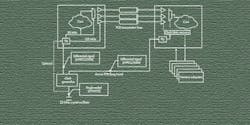
The figure illustrates another PCI Express power reduction option: reference-clock distribution. Here, low-voltage signaling, such as low-voltage positive-emitter coupler logic (LVPECL) and low-voltage differential signaling (LVDS), can be used with reference-clock buffers to reduce power consumption.
Table 1 describes the different multi-level power modes: system, device, link, and physical layer (PHY). By managing these control signals, engineers can make power/functionality tradeoffs from fully working (or on), to optional phase-locked loop (PLL) modes, to system off.
The PCI-SIG recently announced the L1 substates engineering change notice (ECN) (Table 2). This ECN defines additional power states that give designers more options to reduce idle-power consumption. PCI Express L1 substates can significantly reduce idle power, but the tradeoff is latency. The key point is that the power consumption can be reduced from 300 µW to 10 µW.
DDR/LPDDR Power-Reduction Options
New power-reduction options are also available for DDR/LPDDR designs. To see how reducing the supply voltage can have power-saving advantages, compare DDR2 memory to DDR3 memory, which uses 30% less power. This reduction comes from the difference in supply voltages: 1.8 V for DDR2 versus 1.5 V for DDR3.
LPDDR is another common low-power application requirement. LPDDR3 is the next emerging low-power memory standard for mobile applications such as smart phones, and it offers greater bandwidth and higher memory capacity than previous generations of LPDDR. It is projected to achieve data rates of up to 1600 Mbits/s in point-to-point systems using key techniques including write leveling, command/address training, optional on-die termination (ODT), and low I/O capacitance. In fact, activity is under way to update the LPDDR3 standard for data rates up to 2133 Mbits/s. LPDDR3 supports both package-on-package (PoP) and discrete packaging types.
From a DDR design perspective, power can be reduced by up to 60% if the SoC designer can apply the following techniques to the design:
- Avoid the requirement for parallel termination by using short nets and carefully designed DDR PHYs and packages.
- Shut down receivers and transmitters when they aren’t in use, ideally automatically.
- Provide flexible output impedance for maximizing signal integrity but not overdesigning the system.
- Optimize power for DLL, PLL, and I/O for a particular frequency range.
- Reduce delay-line granularity (limit frequency range).
- Keep the system cool by allowing the SDRAM to stay in the “standard” operating range, which requires less frequent refresh operations.
- Simplify the output driver.
- Implement low-power modes. Also, support all refresh modes and partial array self-refresh.
While multiple levels of power-reduction techniques are available, performance must not be affected. Additional techniques to consider include static voltage scaling (SVS), dynamic frequency scaling, retention, hybrid-mode transmitters, bifurcation, and clock distribution. For enterprise systems, PCI Express 3.0 channel loss and the levels of equalization need to be balanced with power consumption. For tablet (mobile) link and power states, new ECNs for L1 substates are driving low-power-use models. With respect to high-speed memory interfaces (DDR), the I/O voltage is a key consideration along with a properly designed system to maximize signal integrity without the use of termination, if possible.
Reference
“Design Custom Chips That Maximize Battery Life,” Electronic Design, May 8, 2012.
About the Author
Navraj Nandra
Navraj Nandra is the senior director, marketing, of the DesignWare Analog and MSIP Solutions Group at Synopsys Inc. He joined Synopsys in February 2005 and has worked in the semiconductor industry since the mid 1980s. He holds a master’s degree in microelectronics, majoring in analog IC design, from Brunel University and a post-graduate diploma in process technology from Middlesex University.
Comment About the Article
To join the conversation, and become an exclusive member of Electronic Design, create an account today!

Leaders relevant to this article: