Understanding ESD And EOS Failures In Semiconductor Devices
Static electricity can be defined as a stationary charge that builds up on the surface of a material. The interaction between stationary charges, known as electrostatics, leads to two key problems: electrostatic overstress (EOS) and electrostatic discharge (ESD).
This file type includes high resolution graphics and schematics when applicapable.
Table Of Contents
- ESD Background
- Charge Generation And Transfer Mechanism
- Electrical Overstress
- Electrostatic Discharge
Typically, ESD causes more than one-third of the field failures in the semiconductor industry. ESD-induced failures in semiconductors can be seen in the form of leakage, short, burnout, contact damage, gate oxide rupture, and resistor-metal interface damage. CMOS scaling reduces power and increases speed, but smaller size increases susceptibility to damage of the thin gate oxide due to EOS/ESD conditions.
The shrinking size of semiconductor chips, thin gate oxides, multiple power supplies, chip complexity, and high-speed circuit operation all contribute significantly to ESD sensitivity. Shrinking gate oxide thickness needs less voltage to be damaged.
Related Articles
- Harvesting Power Using Triboelectric Generators
- The Use And Misuse Of Circuit Protection Devices
- Protect Your Fortress From ESD
It’s tedious to predict ESD because ESD phenomena happen on both a microscopic and macroscopic physical level. ESD protection design is a major challenge for IC designers. With advances in technology at deep submicron levels and to achieve higher quality standards, advanced predictive and robust models with enhanced CAD flow design verification are required to deal with ESD.
ESD damage occurs when people, robotic arms, and other equipment in manufacturing environments handle devices. It also comes from the charge storage of the package itself. ESD is a subset of EOS. IC failures due to ESD can be reduced by two ways:
• Ensure the proper handling and grounding of personnel and equipment during the manufacture, transportation, and application of the IC.
• Add protection circuits to the pins of a packaged IC to divert high currents away from the internal circuitry and clamp high voltages during an ESD stress event.
The ESD protection circuit is designed to turn on in response to an ESD event, clamping the voltage at the bond pad.
Failure analysis of field return devices can assist the design and development process by revealing the failing mechanisms. Chip manufacturers follow the industry standard to qualify their products for ESD. However, they do not have control over a customer’s handling, so effective on-chip circuit protection and testing is desirable.
Charge Generation And Transfer Mechanism
There are three main charge-generation processes: triboelectric charging (contact and separation mechanism), induction, and conduction.
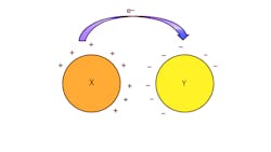
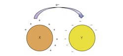
A charge imbalance of e– on the surface of the material due to the friction between different materials is called triboelectric charging. The polarity and strength of the charges produced depends upon the triboelectric properties of materials, surface roughness, pressure applied, temperature, strain, and other factors.
Figure 1 shows the charge transfer from two different electro-negative objects, X and Y. Lets assume when there is contact (friction) between objects that object X loses e– and object Y gains e–. Hence, object X will be positively charged compared to object Y. This phenomenon is known as triboelectricity.
When a person walks across the floor, the contact and separation between the floor and shoe soles generates static electricity. A person walking across a carpet may build up a charge of many thousands of volts, enough to cause a spark. Charge balance is restored through a discharge to the ground. The discharge is extremely fast, on the order of nanoseconds. Generally, people need about 3 kV to feel the shock through static discharge. ESD events usually mildly shock people. But if the same amount of ESD stress is injected into devices, it could be detrimental.
Low relative humidity in the ambient air increases the voltage at which electrical discharge occurs by increasing the ability of the insulating material to hold charge. By decreasing the conductivity of the air, it’s also difficult for the charge buildup to dissipate gradually. Car travel can lead to a buildup of charge on the driver and passengers due to friction between the driver’s clothes and the leather or plastic interiors inside the vehicle. This stored charge is relaxed as a spark to the metal car body while making contact.
Triboelectric charging also happens when an IC slides during shipping tube static electricity is generated due to friction between the tube and lead of the IC. In a normal day, a person generates huge amounts of static electricity. The following list classifies materials on the basis of the triboelectric properties of materials from positive to negative.
- Dry air
- Bakelite
- Glass
- Mica
- Human hair
- Nylon
- Silk
- Wool
- Fur
- Aluminum
- Paper
- Cotton
- Polyester
- Teflon
Other than triboelectricity, electrostatic charge can be generated in material by induction and conduction. A charged material has an electrostatic field. When any conductive material enters the electrostatic field, an internal charge distribution takes place due to induction. Figure 2 shows when an uncharged body B is brought close to a charged body A, and B gets a distributed charge. The near end has a negative charge while the far end has a positive charge. The ESD-Charge Device Model (CDM) is based on electrostatic induction.
When two charged bodies of different electric potentials are brought in contact with each other, charge flows from the higher-potential body to the lower-potential body until both have the same potential. This mechanism is known as conduction.
Broadly, materials can be classified in ESD handling categories such as insulator (ρ > 1012 Ω/square), slow charge dissipative anti-static (109 < ρ > 1012 Ω/square), charge dissipative anti-static (106 < ρ > 109 Ω/square), and conductive (ρ < 106 Ω/square). Anti-static material resists tribocharging, so anti-static and dissipative materials are used to limit charge buildup in manufacturing and assembly environments.
EOS is a term used to describe the thermal damage that may occur when an IC is subjected to a current or voltage that is beyond the datasheet specification limits of the device. An EOS event can degrade the IC or cause permanent functional failure. EOS is a much slower phenomenon than ESD, but the associated energy is very high.
The thermal damage is the result of the excessive heat generated during the EOS event. The high currents in an EOS event can generate localized high temperatures in the low-resistance paths. The high temperature damages device materials such as the gate oxide and interconnects, causing metal burnout. EOS and ESD generally are categorized as a single-term failure mechanism, i.e., “ESD and EOS,” because of the similarities in EOS and ESD failure modes.
ESD and EOS are similar when it comes to stress events, but current or voltage and time stress conditions are different. ESD is a very high-voltage (>500 V) and moderate peak current (~1 A to 10 A) event that occurs in a short time frame. EOS is a lower-voltage (<100 V) and large peak current (>10 A) event that occurs over a longer time frame. Latchup also can cause EOS damage if it persists over a long time.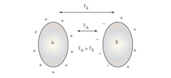
ESD is a transient discharge of static charge between two objects at different electrostatic potentials either through direct contact or an induced electric field. It is the result of a static charged object. Discharging electrostatic charge through an IC creates a large current flow and energy dissipation, damaging the IC. Charge on the surface of any material generally is neutral. When energy is imparted to it, a charge imbalance occurs.
Conductors can’t be charged easily through friction due to high e– mobility in the conducting surface, so charge recombination takes place and preserves the neutral surface. On the other hand, insulators can be easily charged by friction. Imparting energy to non-conducting material results in a large local buildup charge until it is discharged via an external path. Main sources of static electricity include insulators such as plastic surfaces, insulated shoes, wood materials, and bubble pack. Due to non-uniform charge distribution in insulators, voltage levels generated by these sources can be very high, reaching kilovolt totals.
ESD damage in ICs also can come from thermal phenomena. Lots of heat is generated in a localized volume with a very fast rate that is too fast to remove. Thus, ICs get damaged in the form of metal interconnect burnout, poly damage, gate oxide rupture or breakdown, contact spike, or junction breakdown.
When people walk on a synthetic floor, they can accumulate up to 20 kV. Rubbing (friction) nylon and polyester in dry air can produce 25 kV. When a person touches a grounded object, the charge moves from the person to the object in a very short time (1 to 100 ns). The discharge time and current depend upon the time constant.
Discharging current can total approximately 1 A to 10 A. Electrostatic damage to electronic devices can occur at any point from factory to field. Semiconductor devices are designed for ESD protection to withstand high currents for a short time. For example, if a device is qualified for ESD-HBM to tolerate 2-kV specified voltage, then the device can carry 1.3 A with a rise time of 10 ns and a decay time of 150 ns. However, this same device could not carry 100 mA for several milliseconds.
If a device is exposed to a weak ESD pulse and is partially damaged, it may continue to function well enough and pass production automated test equipment (ATE) tests meeting datasheet specifications. The defect may then extend over time with the device failing after several hours. These kinds of defects are known as latent defects, and failures are known as latent ESD failures. Latent defects are hard to detect, especially after the device has been assembled into a finished product.
This file type includes high resolution graphics and schematics when applicapable.

About the Author
Sanjay Agarwal
Sr. Product Engineer
Mr. Sanjay Agarwal is working as Sr. Product Engineer in Timing Solution, Cypress Semiconductor, Bangalore. Mr. Sanjay Agarwal holds a Master of Technology degree from Indian Institute of Technology Kanpur specialized in Electronic Materials, device fabrication and characterization. He has authored numerous technical articles in semiconductor electronics publications.
Comment About the Article
To join the conversation, and become an exclusive member of Electronic Design, create an account today!

Leaders relevant to this article: