Understanding Low-Power IC Design Techniques
Low-power IC design techniques have been around for quite a while. They weren’t always required, though they were nice to have. The rapid growth of the consumer market for battery-powered devices has changed that. Today, low-power design is necessary for gaining and keeping market share. EDA vendors now offer low-power optimization tools, and device modelling has evolved to make more accurate power consumption predictions.
Table of Contents
• Catalyst For Low-Power, Low-Voltage Development
• Industrial Cross-Fertilization
An IC’s total power consumption comprises two types, static and dynamic. Static power typically comes from leakage current and dc current sources. Dynamic current consumption, which is frequency-dependent, often dominates total power. It comes from the charging and discharging of capacitive nodes and the crowbar action of switching transistors connected between the supplies.
Related Articles
- Fundamentals Of Low-Power Design
- Take Simple Steps Toward Extreme Low-Power Design
- Voltage-Drop Analysis Technique Optimizes MTCMOS Cell Placement For Low-Power Designs
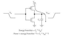
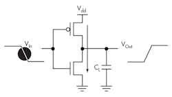
Figure 1 shows the capacitive charge characteristics of the common CMOS inverter. The dynamic charging causes power consumption to be directly proportional to the clocking frequency. Figure 2 shows the crowbar effects. Power is consumed because of the momentary current flow that occurs when both transistors conduct during a logic transition.
The general aim of the low-power designer is to reduce current consumption by minimizing the supply voltage, circuit complexity, clocking frequencies, dc current source values, and capacitance of switching nodes. Circuit functions that are continuously in operation are best implemented in analog circuitry. An analog designer’s approach to low power typically involves:
• Implementation in low-threshold CMOS technologies
• Holding CMOS transistors in the weak inversion (subthreshold) region
• Innovative circuit techniques for complex functions
• Voltage and/or current regulation circuits
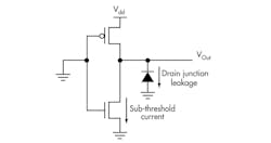
Weak inversion design enables operation at very low supply voltages (Vt + 200 mV) for minimal leakage and switching currents. It’s best suited to low-frequency applications. With the weakly inverted channel of the MOS transistor, typically up to 100 mV below the extrapolated threshold voltage, sub-threshold operation causes a weakly inverted channel of negligible minority carriers to form beneath the gate under moderate electron energy band-bending conditions (Fig. 3).3
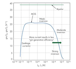
Also, gate-induced band bending in the channel in the absence of significant minority carriers causes the diffusion component of drain current (ID) to dominate the drift component, which approximates to bipolar characteristics. The transconductance (Gm) of MOS transistors working in weak inversion is independent of process spread but dependent upon current and temperature.
Designing large area and long channel devices statistically averages out the effects of surface states. Designing long channel devices minimizes threshold voltage sensitivities to drain source voltage fluctuations. An input switching window of 30 to 40 mV around dc bias can cause the output of a CMOS inverter working in the weak inversion region to fully switch between supply rails. And, MOS output impedance in the saturated region is typically 5 MΩ.
Engineers use these sub-threshold characteristics to full advantage when designing for low current consumption. Furthermore, the ability to detect small signals in the presence of noise improves with increasing power and frequency. Low-power operation therefore places a limit on the minimum detectable signal level and requires specialist design skills for minimizing circuit noise.
Ultra-low-power design skills were initially developed in the Swiss watch industry for maximizing the benefits of using analog circuitry for low-power continuous time applications such as the electronic circuit for sustaining quartz stabilized oscillators.
Event-triggered functions that have relatively long inactive periods are often implemented in the digital domain with a power management function for greater accuracy. A digital designer’s approach typically would include:
• Efficient synthesis of high-level abstraction to logic gate level
• Implementation of multi-level thresholds
• Multiple-frequency clock source
• Novel logic reduction techniques
• Customized level-shifting cells
• Optimized voltage domains
• Power management (power cycling, clock gating)
Catalyst For Low-Power, Low-Voltage Development
In the 1960s, the Swiss watch industry, a significant wealth generator for the local economy, found the nature of the business was changing from mechanical to electronic products with a corresponding fall in price. The Federation of the Swiss Watch Industry (FH) then intensifies its research into electronic timepieces.
Since the electronic quartz clock had already been invented, the challenge was to reduce its power consumption. The Swiss Laboratory for Watch Research (LSRH) in 1962 set up the Centre Electronique Horloger (CEH) joint research laboratory in the LSRH building in Neuchatel to develop the electronic quartz stabilized wristwatch.
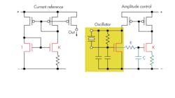
Eric Vittoz, working in Neuchatel at CEH, achieved a breakthrough in low-power design by operating CMOS transistors in their hitherto unknown sub-threshold region. His first paper was presented at ESSCIRC’76, and his patent for amplitude regulation of the 32-kHz oscillator circuit for minimal operating current became an industry standard for quartz stabilized timepieces (Fig. 4).
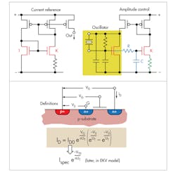
The sub-threshold region before then was regarded as an undesirable characteristic of MOS transistors that appeared as a dc leakage current in CMOS digital circuits. As such, it had not been fully investigated (Fig. 5).
Ebauches Electronique SA bought a CMOS license from Hughes Aircraft to set up EM Microelectronics (Swatch Group) to design and develop ICs for the watch industry. It delivered its first CMOS circuit in 1975 and was instrumental in creating the necessary conditions for the emergence of an industrial-scale low-power, low-voltage expertise.
These events caused the Swiss semiconductor company Faselec to switch from bipolar to CMOS technology for the design of ultra-low-power integrated watch circuits based on Eric Vittoz’s work.
At about this time, Jean Hoerni, a Swiss national and inventor of the planar fabrication process for silicon technologies at Intersil, set up Eurosil electronic GmbH in Munich to exploit the planar process for low-power CMOS applications. This was in direct competition to EM Microelectronics and Faselec. To circumvent Vittoz’s patents, voltage regulation was used that was later complemented by an alternative amplitude regulation circuit using the back gate bias effect.
In 1983, CEH was merged into the Swiss Centre for Electronics and Microtechnology (CSEM), from which the ultra-low-power fabless semiconductor company Xemics (recently acquired by Semtech Inc.) was spun out in 1997 specializing in battery-powered sensor and wireless transceiver applications.
A major Swiss medical OEM in the business of innovative personal hearing equipment has been the main beneficiary of this wireless expertise. Swiss low-voltage, low-current know-how for battery-powered circuits has since helped drive the semiconductor business in battery-powered wireless consumer products.
Industrial Cross-Fertilization
Watches have played a pioneering role in bringing key technologies to industrial maturity and to consumer awareness. There has been a cross fertilization of technology between the watch-making industry and the microelectronics industry.
A watch circuit’s power budget is split between the oscillator block and stepper motor. An integrated stepper motor driver developed in the 1980s for the watch industry uses back-EMF (electromotive force) sensing techniques to minimize current consumption. This adaptive motor drive technique, which extends battery life, now benefits hard-drive stepper motor products for laptops and tablets.
In the late 1980s, semiconductor companies in the watch, clock, and calculator businesses began to turn their attention to radio-frequency identification (RFID) tagging technologies. Subsequent groundbreaking work produced the first prototypes for the American Veterinary Industry in the early 1990s.
At about this time, smart-card patents began to expire, leaving a cost-effective route into a business dominated by Gemplus (France), a company without low-power design expertise. This opened up entry into the contactless RF smart-card business, which coincided with the advent of radio-controlled precision timekeeping watches. Both of these products require ultra-low-power RF design techniques.
Mobile phones, hitherto large and cumbersome, also began to benefit from low-power design techniques. The real-time clock (RTC) used to initiate sleep-mode during inactive periods is based on the 32-kHz quartz crystal watch circuit. Concurrently, battery technology improvements accelerated the miniaturisation process and battery life of these products.
The increasing implementation of RF front-end circuits in CMOS technologies mirrors the switch from bipolar to CMOS of the Swiss semiconductor industry in the late 1970s. The standard CMOS processes of today offer low-threshold voltage options that are comparable to the pioneering low-threshold technologies of the watch industry in the early 1980s. Both Bluetooth and ZigBee have benefited from this development by creating single-chip, low-cost, and low-power communication products.
Due to their confined space, assembly manufacturing techniques such as flip-chip assembly have improved to accommodate slimline watches. Space-saving technologies such as silicon-based microelectromechanical systems (MEMS), critical for adding new functions and increasing the miniaturization of mechanical parts of watches, have fed into new product areas such as RFID transponders, mobile phones, and, more recently, implantable medical devices.
This has enabled the miniaturization of better, unobtrusive hearing aid products (MEMS-based hearing aids) that are cheaper and offer longer battery life. The next generation of active implantable drug delivery systems for the controlled release of drugs to affected areas likewise will be based on MEMS technology.
Standard semiconductor processes are now suitable for specialized low-power applications in the emerging market for implantable medical devices. An ultrasonic pacemaker with a transceiver implant developed by Cambridge Consultants for EBR Systems eliminates pacing leads and the need for invasive surgery by stimulating the heart through wireless transmission of energy to an implanted electrode.
Energy harvesting techniques are synonymous with low-power requirements. Kinetic energy conversion and wireless power transmission techniques, first pioneered in the watch and RFID industries respectively, are becoming increasingly attractive as alternative sources of power for implantable equipment.
The two-year SIMM (self-energizing implantable medical micro system) project is developing an in-body micro-generator that will convert kinetic energy from human body movement into power for implanted medical devices including pacemakers, electrical stimulators, and body area network applications.
Deep in the inner ear of mammals is a natural battery, a chamber filled with ions that produces an electrical potential to drive neural signals. Massachusetts Institute of Technology (MIT) researchers have identified this chamber as another potential energy source for powering implantable electronic devices.
A former MIT graduate student, Patrick Mercier, who is now an assistant professor at the University of San Diego, helped develop an integrated radio transmitter circuit at Microsystems Technology Laboratories of MIT (MTL) powered by this biological battery without causing any hearing loss.
The application of microsystems technology to the emerging field of nanotechnology is making the unthinkable of a few years ago more of a reality. Research laboratories are working on the use of manufactured nano-robots to make repairs at the cellular level (nano-medicine). Selection of the appropriate energy sources for self-powered nano-systems depends on low-power design.
Low-power design techniques, therefore, are crucial to the successful development of high-tech products for tomorrow’s world.
Medical electronics represents more than 10% of the circa $30 billion global industrial semiconductor market and is the fastest growing market segment with an expected growth rate of 10% per year.
By removing the need for regular visits to the clinic, new application areas in the medical industry for patient implantable sensing devices offer low-cost health-care solutions. This resulting explosive growth in personal battery-powered medical equipment is fuelling the development of micro-powered (wireless) implantable devices for neural stimulation and heart pacing activities.
In recognition of the potential for lower medical costs combined with improved quality of life for patients, European Union funding has been used to develop a range of medical implants that will help patients with specific disabilities relating to the nervous system.
The RFID market today, which includes contactless smart cards, transponder/tagging technologies, and both active and passive RFID with associated readers, is worth over $12 billion. Challenges with tag yield versus cost, frequency acceptance, specification creep, and required performance levels are some of the key issues that are being resolved to grow the RFID market exponentially.
IDTechEx predicts the 2016 value of the total market, including systems and services, will rocket to $26 billion. This includes many new markets that are being created, such as the market for real-time location systems using active RFID, which will itself be more than $6 billion in 2016.
The medical industry is the latest market sector to benefit from the Swiss watch industry’s drive toward increasingly lower power and smaller size with greater complexity of functionality and longer battery life. The rapid progress in wireless sensors, continually tracking parameters such as blood sugar, blood pressure, and heart rate, has the potential to advance health and change medicine in a radical and unprecedented way.
Accurate and timely detection of medical conditions is critical for initiating effective treatment. Low-power implantable medical device technology will enable the universal adoption of accurate real-time monitoring of patients and localised delivery of the appropriate remedy.
1. Solid-State Circuits Society, “The Electronic Watch and Low Power Circuits,” Eric Vittoz, summer 2008
2. MIT News, “Medical devices powered by the ear itself,” November 7, 2012
3. "Optimizing analog IC designs when every nanoAmpere counts," Pablo Aguirre and Fernando Silveria, EDN, July 17, 2012

About the Author
Clive Taylor
Clive Taylor works in medical electronics at Cambridge Consultants, Cambridge, U.K. He has more than 30 years in the semiconductor industry with 10 patents in low-power IC design. Specifically, he has eight years in the watch/clock/solar-powered calculator/RFID industry with Eurosil electronic GmbH, Munich; seven years at VLSI Technology Inc., Milton Keynes, U.K., working on Ericsson mobile phones including Bluetooth development; two years at Jennic, Sheffield, U.K., working on ZigBee; three years at Frontier Silicon, Cambridge, working on the first fully integrated front-end receiver for DAB radio; nine months as a contractor at Broadcom Inc., Cambridge, working on multimedia products for mobile phone products; and six months as a freelance consultant at Semtech Inc., Neuchatel, Switzerland (formerly Xemics), working on wireless battery-powered medical products.
Comment About the Article
To join the conversation, and become an exclusive member of Electronic Design, create an account today!

Leaders relevant to this article: