Use A Flyback Topology To Drive Custom LED Lighting
LED replacement bulbs include integrated driver electronics employing a variety of circuit topologies. But LED light fixtures frequently require standalone LED power supplies, sometimes called modules or bricks, often not produced by the fixture manufacturer. These supplies are available in a wide range of power levels rated at different output voltages and currents to cover many different LED loads.
Related Articles
- Use Flyback Converters To Drive Your LEDs
- Mind The Gap And Improve Your Low-Power Flyback Transformer Design
- Enhance Synchronous Rectification Control In Flyback Converters
LED power supplies for light fixtures typically fall within in the 30- to 60-W power range, generally requiring isolation, constant output current, a wide input voltage range, high power factor and low total harmonic distortion (THD), short-circuit and open-circuit protection, and electromagnetic interference (EMI) compliance. Dimming by 0- to 10-V control also may be required.
The flyback topology enables a cost-effective platform to provide the desired functionality. This type of converter is based around a control IC. Several types of control ICs are available. These devices include functionality specific to the LED driver in addition to basic switch-mode power supply (SMPS) control. They also vary in associated system complexity, cost, and ease of use. A good control IC to base a design on simplifies the design process through its versatility and ease of interface with surrounding circuits.
This file type includes high resolution graphics and schematics when applicable.
Background
Before discussing the circuit design, it should be recognized that a critical factor in creating as efficient a flyback converter as possible is the design of the transformer, which is in fact a coupled inductor. It is necessary to minimize conduction and core losses and essential to minimize leakage inductance, which should be kept below 3% of the actual inductance.
A split primary winding is required to accomplish this, which is constructed by first winding half of the primary on the inside of the bobbin and then winding the secondary and auxiliary windings before finally winding the second half of the primary on the outside. High leakage inductance leads to larger ringing oscillations at the MOSFET drain, creating increased losses in the snubber network that significantly lower the converter efficiency. Efficiency above 85% should be achievable for most converters. This depends largely on load voltage and current. High current outputs produce greater losses in the output diode.
A great benefit of the flyback converter is that it can provide high power factor and isolation in a single conversion stage using a single high-voltage MOSFET. This is done by means of an unsmoothed full-wave rectified primary bus voltage with the converter operating in critical conduction mode (CrCM). The regulating loop speed is slow relative to the ac line frequency so the switching-on time does not vary significantly over the line half cycle.
The input current then can remain approximately sinusoidal, providing a power factor above 0.9 over a wide input voltage range with a THD under 20%. Output current must be smoothed by capacitors placed at the output to reduce the low-frequency ripple to an acceptable level. There is a tradeoff between ripple and capacitor size that typically results in ripple in the region of 20%, which does not produce visible flicker in LEDs.
One very important issue in LED drivers is that light output should appear within half a second of applying ac power. Longer switch-on delays are objectionable to most end users accustomed to the almost instant response of the filament lamp.
Some IC controllers such as the IRS2983 accomplish rapid start by means of an on-board high-voltage startup circuit. This circuit is connected to the rectified dc bus to supply a current to VCC at switch-on, enabling the VCC capacitors to charge rapidly and allowing the system to start up. This avoids the need for startup resistors that waste power and introduce noticeable delay on startup at low line voltages.
Current Regulation Methods
The first and simplest method uses primary-side regulation. Several LED controller ICs can regulate the LED output current within ±5% over a wide input voltage range. This is done without the need for any feedback loop, so no opto-isolator is required. Control methods vary between different parts. Some provide current regulation for a fixed load, and some can also accommodate some load voltage variation.
Primary regulation operates from states such as the line input voltage, MOSFET current, and de-magnetization voltage that can be sensed from the primary side of the converter. These quantities are used to approximate the output current or power. If the output voltage is fixed, the input power is approximately proportional to the input power and can be used to provide regulation.
Open circuit protection is usually provided through the zero-crossing or de-magnetization input, which senses the zero crossing point for the transformer and the reflected voltage shutting off the gate drive if it becomes too high. This way, output components are protected from over-voltage without the need for direct sensing.
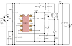
Short-circuit protection is provided by collapse of the VCC supply since the auxiliary transformer winding loses voltage when the secondary side is short-circuited. This causes the IC to shut down and then to restart through the high-voltage startup circuit. This cycle continues in hiccup mode until the short circuit is removed (Fig. 1).

The second method, which uses a feedback loop with an opto-isolator, is more complicated and requires more components. It can provide a very accurately regulated output current over a wide output voltage range. While the first method suits fixed-load LED drivers, the second fits drivers that can operate with a range of different loads with the same current rating.
The opto-isolator connected to the control IC provides isolated feedback. In the following example, the control IC is configured for closed-loop operation by connecting the input voltage sensing input to 0 V. The COMP pin then becomes a current source connected to the collector of the opto-isolator transistor. The voltage at this pin determines the switching-on time and therefore controls the output current. The output current and voltage are sensed and compared with a reference by circuitry located at the output side. The error signal drives the opto-isolator to close the loop.
The feedback circuit uses an op amp to amplify the dc output current sensed by the shunt resistor ROUT. This allows current sensing with minimal power loss. The developed voltage is amplified so that at the regulated current, the op-amp output reaches the reference level of IC3, a TL431 low-cost but very accurate device with a 2.5-V reference that behaves somewhat like a zener diode.
Loop compensation is provided by the network RP and CP to roll off the gain below the ac line frequency necessary for maintaining a high power factor. A capacitor at COMP is also required to remove noise, which can be 0.1 µF. If the loop speed is too slow, a large current transient occurs at the output at switch-on. If it is too fast, the power factor is degraded.
Over-voltage protection is added by means of DOV and ROV. DOV is a zener diode rated a little above the desired over-voltage shutoff level such that under open circuit conditions, this diode will conduct and force the op-amp output high, driving the COMP pin low through the opto-isolator IC2 and shutting off the gate drive.
Since the ZX input of IC1 is not used in this case for over-voltage protection, a 3.9-V zener diode DCOMP is added to clamp the de-magnetization signal below the ZX protection trigger threshold. This is done to allow the ZX detection to operate over a wide output voltage range without the risk of falsely tripping the ZX protection or missing cycles at low line when the output voltage is low.
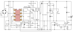
IC4 is a low-cost op amp such as an LMV321, which requires a 5-V supply and can operate down to 2.7 V. For the secondary-side circuitry to operate under short-circuit conditions or with very low-voltage LED loads, a dual-supply circuit is implemented for the op amp and opto-isolator. Under normal operating conditions, the supply is derived from the output through a simple voltage regulator built around QVSN.
The base of this NPN transistor is biased at one diode drop above QVSS so QVSS conducts only when the collector supply to QVSN has fallen below the zener voltage of DDS plus the forward drop of DDS. The collector of QVSN is supplied from the forward phase of the flyback converter, which provides a voltage on CF. This relatively high voltage varies considerably with ac input voltage, so it does not offer an efficient means of supplying the secondary side circuitry. This alternative supply, then, is used only as a backup when the output voltage is not available.
Hot reconnect is sometimes required in LED drivers, meaning the load can be disconnected and reconnected and continue operating normally. This is more problematic than it may initially appear because when the load is disconnected, the output capacitors CVOUT charge to the over-voltage protection level, which may be significantly higher than the rated load voltage.
Discharging a large capacitor through an LED load creates a very high current transient that can destroy the LEDs. To add some protection against this, an NTC thermistor has been added at the output. It advisable, however, to avoid hot reconnecting of LED loads wherever possible!
As in all switching converters, an EMI filter is necessary at the input. This is based on a standard configuration to attenuate both common-mode and series-mode components of conducted interference below the limits specified by the applicable standard.
CX1 and CX2 are normally equal and should not be too large to maintain the best possible power factor. Since these capacitors introduce phase shift, the larger they are, the more they will reduce the power factor particularly at high line. LF1 and LF2 may be increased as required provided the current rating is sufficient for the converter input current at low line voltage and full load. In some cases, a common-mode choke may be used in place of LF1 and LF2 or even in addition to them if necessary.
Flyback converters generate more emissions than some other topologies due to the asymmetry, ringing, and high dv/dt of the drain voltage. Common-mode noise depends on leakage to earth, which depends partly on PCB layout and transformer construction. CY1 and CY2 are used for further attenuation of common-mode noise, though they require an earth connection, which is not always available and may not be too high since standards do not permit ground leakage exceeding a small amount. This is important to avoid false tripping of ground fault interrupt (GFI) types of protection breakers.
In addition to EMI emissions, immunity should be considered. Both circuits presented include a varistor or voltage-dependent resistor (VDR) connected at the ac input. This is essential to absorb the energy from surges that often appear on the line and can damage the MOSFET or IC if no protection is added. The VDR alone is not sufficient to protect the circuit against surges above 1 kV.
Since the one-stage power-factor correction (PFC) flyback circuit has no dc bus bulk capacitor, there is nothing to absorb a high-voltage surge except for the VDR. Depending on the level of protection required by the application, an additional transil diode may be added across the dc bus. This device acts like a zener diode clamping voltage but can absorb much more energy. A 0- to 10-V controlled analog dimming circuit can be added to the circuit by replacing IC3 with a second op amp (Fig. 3). Isolation already exists at the output, making it convenient to reference the dimming circuitry to the secondary output.
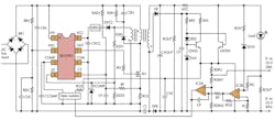
The 0- to 10-V control voltage provides a reference for the current regulation loop so that as this voltage level is reduced, the output current reduces by a proportional amount. IC3 and IC4 are replaced by a dual op amp, which can be a low-cost standard part such as an LM358. The 0- to 10-V dimming system operates by sinking current from an external dimmer or controller, which requires each LED driver to produce a supply voltage a little over 10 V. For this to work, the supply voltage to IC3 can be increased to 12 V by changing DVS.
The values of RDIM1 and RDIM2 are large compared to RDPU, which should be large enough to limit the maximum current sourced by the 0- to 10-V control input if it becomes short circuited to a small around 1 mA. This will not pull down significantly on the secondary VCC supply. RDIM1 and RDIM2 form a divider to scale the reference voltage to match the output voltage of IC3B at maximum output current. Loop compensation is now placed around IC3A. A simple dimming scheme as described can provide stable and linear dimming response over a wide range of ac line input voltage typically down to 5% or lower for a fixed load.
Dimming becomes more complicated if it’s required to work over a wide range of line and load. This may prove to be impractical due to the limit of dynamic range available in the flyback converter.
Some control ICs can operate in discontinuous conduction mode under light load conditions such as during dimming. The gate drive then can operate with a very small duty cycle, which would not be possible if the system were still working in critical conduction mode. An IC incorporating this feature should be used for the controller in a dimmable LED driver design.
Whatever variation of the circuit is used, the selection of components determines the thermal performance of the system. A power supply for a lighting application should avoid any component exceeding 70°C in open air after settling at maximum temperature. This will prevent poor reliability and can allow operating life up to 25,000 hours, provided high-temperature-rated long-life electrolytic capacitors are used. Typically, the components that run hottest are resistors, the output diode, the snubber components, and the MOSFET.
For designs where the output current exceeds 0.5 A, a small package output diode (DFB) inevitably exceeds the desired temperature. It is often necessary to use a larger package such as a DPAK or even TO-220 to avoid this. The MOSFET should also be selected with low enough RDS(on) to avoid high running temperature, and the transformer should be large enough to accommodate conductors large enough to keep the resistive losses low.
Conclusion
The flyback LED driver platform offers many benefits without excessive cost. Designers can create a successful design by accounting for the performance factors explained above. The general design flow will be:
• Specification
• Select basic design (Figure 1) or advanced design (Figure 2 or 3)
• Design transformer
• Select components
• Design EMI filter
Design tools are available to aid in calculating the transformer core and wire sizes and turns as well as selecting the correct component values for the circuit. The EMI filter normally requires testing with different filter capacitor and inductor values to arrive at the simplest filter that will meet the required limits. Such bench testing requires a spectrum analyzer and impedance network (LISN) and should be carried out at high line voltage, which is the worst case.
The entire process, as may be expected, usually requires some iteration before reaching an acceptable tradeoff between performance, power factor, THD, and EMI. Fortunately, many excellent application notes and design tools are available to aid the designer.

About the Author
Peter Green
LED Group Manager
Peter Green is the LED Group manager, energy saving products, at International Rectifier Corp. He received a BSc in electrical engineering from Queen Mary College, University of London, in 1985. Since then he has worked in product design and development for commercial and military companies in the power supply and lighting industries in the U.K. He is a member of the Institution of Engineering and Technology and a Chartered Engineer. In 2001 he relocated to California to join the Lighting Design Center at International Rectifier, where he has worked on new lighting ASIC definition and design, as well as application support. He is currently managing LED systems and applications. He has previously presented at APEC, PCIM, and many other conferences and has several patents related to lighting electronics. He can be reached at [email protected].
Comment About the Article
To join the conversation, and become an exclusive member of Electronic Design, create an account today!

Leaders relevant to this article: