WBG Power Transistors Push the High-Power Envelope
This file type includes high resolution graphics and schematics when applicable.
Early predictions of widespread dominance were somewhat premature, but over the next several years, wide-bandgap (WBG) devices using gallium-nitride-on-silicon (GaN on Si) and silcon-carbide (SiC) process technologies are expected to gradually replace traditional Si MOSFETs in many power applications. Transistors made with another WBG semiconductor—carbon in the form of synthetic diamond— hold even more promise, but production is still several years away.
The performance improvements of these materials don't come without a cost, though. Packaging designers in particular face new challenges in making the most out of these materials. Let’s take a look at some recent developments in power transistors and high-power packaging technology.
WBG Technology Overview
If it's been a while since your last solid-state physics class, here's a quick review. The bandgap of a solid is the energy range that’s devoid of electron states. Its width is measured in electron volts (eV) and indicates the energy difference between the top of the valence band and the bottom of the conduction band; it's a major factor in determining a material's electrical conductivity.
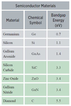
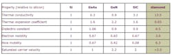
As shown in Table 1, silicon has a bandgap of 1.1 eV, but WBG semiconductor bandgaps range from 3.3 to 5 eV. The wider bandgap means that more energy is required to move an electron from the valence band to the conduction band. Table 2 provides a relative comparison of some key WBG properties compared to silicon.
As far as real-world performance is concerned, the wide bandgap brings a number of benefits:
• WBG unipolar devices are thinner and have lower on-resistance. This also means lower conduction losses, allowing for higher overall converter efficiency.
• WBG power devices have higher breakdown voltages—Si Schottky diodes exhibit breakdown voltages lower than 300 V, while commercial SiC Schottky diodes currently boast numbers of 1700 V or higher.
• WBG devices have a higher thermal conductivity, so WBG-based power devices have a lower junction-to-case thermal resistance (Rθjc). This means heat is more easily transferred out of the device, and thus slows down the increase in device temperature. GaN is an exception in this case, since it has a thermal conductivity lower than silicon.
• WBG semiconductor-based power devices can operate at higher temperatures. SiC devices will operate up to 600°C, and GaN may extend beyond that. Si devices, on the other hand, operate at a maximum junction temperature of only around 150°C.
• Forward and reverse characteristics of WBG semiconductor-based power devices vary only slightly with temperature and time, so they're more reliable.
• WBG semiconductor-based bipolar devices have excellent reverse-recovery characteristics. Less reverse-recovery current reduces switching losses and electromagnetic interference (EMI), so there’s less need, or no need at all, for snubbers. As a result, soft-switching techniques aren’t required to reduce switching losses.
• Due to their lower switching losses, WBG devices can operate at higher frequencies (>20 kHz) not possible with Si-based devices at power levels of more than a few tens of kilowatts. Higher switching frequencies make it possible to use smaller capacitors, inductors, and transformers, which in turn shrink power-converter size, weight and cost.
What does this mean for power-system designers? Research conducted by Yole Developpement estimates that replacing silicon with SiC or GaN can increase dc-dc conversion efficiency from 85% to 95%; boost ac-dc conversion efficiency from 85% to 90%; and optimize the efficiency of dc-ac conversion from 96% to 99%.
It may not seem like a lot, but a 3% improvement on an EV drivetrain that's switching 100 kW means 3 kW less heat needs to be removed. That translates into smaller cooling systems or radiators.
GaN devices up to 900 V have recently been announced, which will extend their reach into offline converters and power factor correction, both huge markets. Class D amplifiers will also benefit from faster switching speeds, leading to lower audio distortion and reduced filter size.
Both SiC and GaN technologies still have manufacturing issues to overcome, though. For instance, GaN has low thermal conductivity and defect issues, while SiC maintains high wafer costs and low electron mobility.
What about the prospects for diamond? Synthetic diamond produced by chemical vapor composition (CVD) shows great promise as a semiconductor material, with a broad range of desirable properties. Still, it's not quite ready for prime time, with one main obstacle revolving around doping difficulties.
Diamond transistors are the subject of much active research. In 2013, for example, researchers at the Tokyo Institute of Technology reported fabrication of a JFET with a breakdown voltage of 566 V at room temperature, and over 600 V at 208°C. Last year they achieved 1530 V with a MESFET device.
The material needed for production parts is moving closer to fruition, though. Illinois startup AKHAN Semiconductor is developing diamond wafers using a microwave plasma-assisted CVD process (MPCVD) and technology licensed from Argonne National Laboratory's Center for Nanoscale Materials.
Recent WBG Products Push the Envelope
A stream of new products helps extend WBG's reach across a broad spectrum. Below are some notable announcements from three of the leading GaN and SiC suppliers.
In high-frequency power electronics, Wolfspeed (formerly Cree), a leading supplier of both SiC and GaN devices, recently introduced the industry’s first 900-V SiC MOSFET platform. Optimized for power applications including renewable-energy inverters, electric-vehicle charging systems, and three-phase industrial power supplies, the company claims the new 900-V platform enables smaller and higher-efficiency next-generation power-conversion systems at a cost equivalent to silicon-based solutions.
The lead product (C3M0065090D) features an RDS(ON) of 65 mΩ (typ), claimed to be the lowest of any available 900-V MOSFET device . In addition to standard TO247-3 and TO220-3 packages, the new device also comes in a low-impedance D2Pak-7L surface-mount package with a Kelvin connection to help minimize gate ringing.
Existing 900-V silicon MOSFETs have high switching losses (due to parasitic capacitances) that increase with frequency. In addition, their RDS(ON) increases three to five times over temperature, which causes thermal issues and significant derating. The Wolfspeed device features an RDS(ON) increase of only 40% from room temperature to Tj = 150°C, enabling a smaller thermal-management system.
Infineon, which acquired International Rectifier along with its GaN platform, recently announced a strategic partnership with Panasonic. It will result in jointly introduced devices utilizing Panasonic’s normally off (enhancement mode) GaN-on-Si transistor structure integrated into Infineon’s surface-mount device (SMD) packages, providing a GaN power device with dual sourcing.
The company is also sampling a 600-V, 70-mΩ, GaN cascode device in a DSO-20 package. At APEC 2015, Infineon demonstrated a 1-MHz LLC converter converting 319 V to 24 V with 96% efficiency. Its 9-mm height suits it for consumer applications such as ultra-thin LED TVs.
In RF power, Qorvo (formed by the merger of Triquint and RFMD) recently announced a number of high-power GaN devices, including multi-stage monolithic microwave integrated circuits (MMICs) and devices in plastic packages. Expanding beyond military and government electronics, the new products target commercial markets such as base stations, point-to-point wireless, cable TV, and VSAT applications.
The new products boost power outputs across a broad range of frequency bands, from dc to Ka band. Power outputs include: 300 W in L band (1-2 GHz); 100 W at S band (2-4 GHz); 50 W at X band (8-12 GHz); 35 W at Ku band (12-18 GHz); and 10 W at Ka band (26.5-40 GHz).
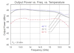
The TGA2239-CP, for example, is a 3-stage, 35-W power amplifier operating over the 13.4- to 15.5-GHz band (Fig. 1). Fabricated on Qorvo's production 0.15-µm GaN-on-SiC technology, the part offers > 30 dB small-signal gain with 34% PAE, and is offered in a 10-lead, 15- x 1- mm bolt-down package with a pure-copper base for superior thermal-management characteristics.
Maximize WBG Advantages with Better Packaging
SiC and GaN devices have the potential to operate at temperatures up to at least 600°C, but multiple packaging components must be optimized to fully utilize their performance. In addition, WBG power devices switch at much higher speeds than equivalent silicon devices, but since they must be supported by silicon drivers and controllers, package parasitics have to be minimized. Accomplishing this feat presents some challenges:
• Interconnects (soldering): Since most current solders are not 200°C-capable, research is focusing on alternatives, including silver nanoparticles. A nanoparticle joint has a high melting point (960°C) compared to the low processing temperature (<300 °C). However, silver migration is a problem that remains to be solved for high-temperature, high-power applications. Solid-liquid inter-diffusion (SLID) bonding also shows promise. This technique utilizes a binary system with one HT melting metal and one LT melting metal; for example, gold and tin.
Copper-wire interconnect is another possibility. It demonstrates higher reliability under thermal cycling due to higher fatigue strength, lower coefficient of thermal expansion (CTE), and much better thermal conductivity. More exotic options for new thermal interface materials include nano fillers, or even carbon nanotubes or diamond films.
• Substrates: Achieving the maximum thermal dissipation requires direct attachment of the heat-generating device to a thermal substrate or package. An HT substrate must also have a CTE matched to those of the attached devices to minimize thermal cycling stress.
Key electrical requirements include high thermal conductivity, high resistivity to reduce leakage, a high dielectric strength to withstand high voltage, and a low dielectric constant to limit common-mode capacitance.
Direct-bonded copper (DBC) substrates are commonly used in power modules due to their high thermal conductivity. They consist of a ceramic tile (AlSiC is promising for WBG use) with a sheet of copper bonded to one or both sides by a high-temperature oxidation process. The top copper layer can be pre-formed prior to firing or chemically etched using standard PCB technology to form an electrical circuit, while the bottom copper layer is usually kept plain. The substrate attaches to a heat spreader by soldering the bottom copper layer to it.
Another possibility is to use advanced printed-circuit-board (PCB) laminate with thicker metal layers. Fraunhofer IZM, for example, reported some promising results by embedding the power devices and passives into cavities in the PCB, and using the copper layers of the laminate for interconnection and heat management.
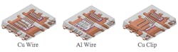
• Parasitics: Much work is being done to reduce inductive and capacitive parasitics. At high switching frequencies, the traditional wire bond can act like an antenna, creating issues with parasitic inductances. Copper pillar interconnects, which use cylindrical copper connections instead of solder bumps for flip-chip assembly, offer superior parasitic performance. Substrate materials, as well as the design and positioning of the components on the substrate, are also keys to reducing parasitics.Three-dimensional packaging is another option—stacking devices reduces electrical parasitics by placing common terminals in immediate contact. Copper clip bonding is the preferred method for connecting devices, since it reduces package inductance and resistance as well as thermal resistance, leading to a higher current rating capability and efficiency (Fig. 2).
The APEI Multichip Power Module
At the module level, the packages themselves must be thin for efficient thermal capability, and have both top-side and bottom-side cooling. Multiple components with different substrate potentials may need isolated package substrates that are electrically isolated but thermally conductive.
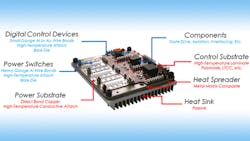
Several competing solutions are under development, but one promising option is multichip, flip-chip packaging, where the driver and the power device can be co-packaged to minimize parasitics. Incorporating many of these concepts is the multichip power module (MCPM) technology developed by APEI, a unit of Wolfspeed (Fig. 3).
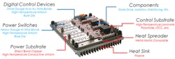
The MCPM integrates the control and power circuitry components into a single power module that’s constructed in two stages.
The first stage consists of a DBC substrate with wide metallization traces designed to conduct high voltages and currents. The high-power, bare-die WBG devices (SiC in this case) are mounted with a high-temperature die-attach method directly to the DBC substrate, providing an excellent thermal path to the heat spreader.
The second stage is the control board. Due to the demanding power and thermal requirements, the power-substrate metallization traces cannot be tightly patterned for high-density control electronics. Instead, the control board is fabricated from a high-temperature multilayer polyamide substrate. The control components are bare-die devices wire-bonded with gold wire, surface-mount passives, and magnetic components.
The control board is mounted to the high-power substrate by a high-temperature adhesive. The heat spreader consists of a metal-matrix-composite material (MMC), which is a ceramic matrix injected with a metal. These heat-spreader materials offer excellent thermal conduction capabilities while providing a close CTE match to the DBC ceramic substrate.
Looking Forward
In terms of market penetration, expectations are that for mid- and high-end designs, GaN will be strongest in lower-power or lower-voltage (200-V) applications, and SiC at higher voltages and powers. Traditional Si devices will still dominate low-end designs.
Costs remain an issue, though. Both super-junction MOSFETs and IGBTs are ramping up on 300-mm wafers, making them less expensive than GaN and SiC. SiC MOSFETs are ramping up on 100-mm wafers, while GaN-on-Si is running on 150-mm wafers.
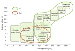
Still, WBGs are steadily finding their way into designs, notably in photovoltaic (PV) power generation, and migrating to more general power-grid applications. Longer term, electric vehicles are expected to be the largest application by 2020. Figure 4 shows Keysight Technologies' view of the WBG application space.
About the Author
Paul Pickering
Paul Pickering has over 35 years of engineering and marketing experience, including stints in automotive electronics, precision analog, power semiconductors, flight simulation and robotics. Originally from the North-East of England, he has lived and worked in Europe, the US, and Japan. He has a B.Sc. (Hons) in Physics & Electronics from Royal Holloway College, University of London, and has done graduate work at Tulsa University. In his spare time, he plays and teaches the guitar in the Phoenix, Ariz. area
Comment About the Article
To join the conversation, and become an exclusive member of Electronic Design, create an account today!

Leaders relevant to this article: