What’s The Difference Between Operational Amplifiers And Instrumentation Amplifiers?

Download this article in PDF format.
The term instrumentation amplifier (INA) often is misused, referring to the application rather than the architecture of the device. Historically, any amplifier that was considered precision (i.e., implementing some sort of input offset correction) was considered an INA, since it was designed for use in measurement systems. INAs are related to operational amplifiers (op amps), since they are based on the same basic building blocks. But an INA is a specialized device, designed for a specific function, as opposed to a fundamental building block. In this regard, INAs aren’t op amps, since they are designed to function differently.
Table Of Contents
• Primary Differences
• Difference Amp
• Two-Op-Amp INA
• Three-Op-Amp INA
• INA And Op-Amp Specifications
• Wheatstone Bridge
• Review
Primary Differences
Perhaps the most notable difference between an INA and an op amp in terms of usage is the lack of a feedback loop. Op amps can be configured to perform a wide variety of functions, including inverting gain, non-inverting gain, voltage follower, integrator, low-pass filter, high-pass filter, and many more. In all cases, the user is providing a feedback loop from the output of the op amp to the input, and that feedback loop determines the function of the amplifier circuit. This flexibility is why op amps are ubiquitous in a wide variety of applications. An INA, on the other hand, has this feedback internally, so there isn’t an external feedback to the input pins. For an INA, the configuration is limited to one or two external resistors, or perhaps a programmable register, to set the gain of the amplifier.
INAs are specifically designed and used for their differential-gain and common-mode-rejection (CMR) capabilities. The INA will amplify the difference between the inverting and non-inverting inputs while rejecting any signal that is common to both inputs, resulting in no common-mode component being present at the output of the INA. An op amp configured for gain (either inverting or non-inverting) will amplify the input signal by the set closed-loop gain, but the common-mode signal will remain at the output. The difference in gain between the signal of interest and the common-mode signal reduces common mode (as a percentage of the differential signal), but the common mode is still present at the output of the op amp, which limits the dynamic range of the output.
As mentioned, INAs are used to extract a small signal in the presence of a large common mode, but this common-mode component can take many forms. When using a sensor in a Wheatstone bridge configuration (which we will explore later), there is a large dc voltage that is common to both inputs. However, interference signals can take many forms. One common source is 50- or 60-Hz interference from the power lines, not to mention the harmonics. This time-varying error source often fluctuates greatly across frequency as well, making it extremely difficult to compensate for at the output of the INA. These variances make specifying CMR important, not only at dc but also across a range of frequencies.
Difference Amp
Designers may ask if they can build an INA out of simple op amps. The short answer is that they can. But there are always tradeoffs! One may first think of a simple difference amplifier circuit, sometimes called a subtractor, that provides for differential gain and has some CMR, which is exactly what an INA is intended to do (Fig. 1). This circuit presents several tradeoffs.
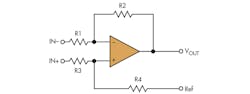
1. Analyzing the limitations of difference amplifiers helps in understanding why it isn’t easy to make an INA out of a handful of op amps.
First, consider input impedance. It is relatively low, as determined by the values of the resistors, which may be on the order of 100 kΩ. Second, the input impedances aren’t matched, meaning a different current will flow through each leg, causing the CMR to suffer. The other shortcoming of this simple circuit is the need for resistor matching. The level of matching within the resistor pairs, not the op amp itself, predominately determines its CMR. Any mismatch in these resistor pairs will reduce the CMR, which can be calculated as:
CMR = 20 log [(1 + R2/R1)/Rt]
Where Rt = total mismatch of the resistor pairs in fractional form. For example, assume R1 = R2 = R3 = R4 (providing unity gain), and the resistor mismatch is 1%. Using the above equation:
CMR = 20 log (1 + 10.01)
CMR = 46 dB
As this example shows, the performance one can achieve with this simple circuit is extremely limited. Even when matching resistors by hand, a CMR any greater than 66 dB will be difficult to achieve. In addition, this does not address fluctuations due to temperature, as any difference in temperature coefficients among the resistors will further increase the mismatch and result in worse CMR. Accounting for all of these factors and limitations, a monolithic difference amplifier is usually the best solution for relatively high-performance applications.
The difference-amplifier circuit discussed previously technically isn’t an INA, but it is useful for certain applications requiring high speed and/or high common-mode voltage levels. For precision applications, an actual INA is often the best choice. Two common circuits are utilized to create an INA, one based on two amplifiers and one based on three amplifiers. Both will be discussed in detail. Note that these basic circuits can be constructed using standard op amps, but they are also the underlying circuit concepts used in many of the monolithic INAs offered today.
Two-Op-Amp INA
This popular INA circuit is based on two amplifiers (Fig. 2). In this circuit, the overall gain is set via one resistor, noted below as RG, such that:
G = 1 + R2/R1 + (2*R2)/RG
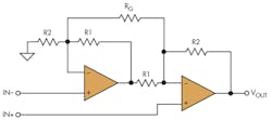
2. In a two-op-amp INA, a single resistor sets gain. Unity gain is impossible, and common-mode range is limited.
One of the limitations of this circuit architecture is that it does not support unity gain. Although most INAs are used to provide gain (and hence unity gain is not critical), some applications specifically use an INA strictly for CMR. So, it is reasonable to assume that an INA may be used in a unity-gain configuration for some applications.
Another drawback of the two-op-amp INA is the input’s limited common-mode range, especially at lower gains and when it’s used with single-supply op amps. Keep in mind that the amplifier on the left-hand side of Figure 2 must amplify the input signal at the non-inverting node by 1 + R1/R2. Thus, if the common mode of the input signal is too high, the amplifier will saturate (run out of headroom on the output). At higher gains, there is more amplifier headroom and the circuit can support a wider input signal CMR, all else being equal.
One of the limitations of the difference-amplifier circuit discussed previously is its low input impedance. The two-op-amp INA circuit does not have this issue, since the two differential input signals feed directly into the input pins of the amplifiers, which generally have impedances in the millions of ohms. But, due to the difference in the input signal paths, there is a delay difference between the differential input signals, which results in poor CMR across frequency—a critical specification for INAs. Similar to the difference-amplifier circuit, the matching of the resistor ratios once again limits the CMR at dc.
A monolithic INA based on this two-op-amp architecture will inherently have better resistor matching and temperature tracking, relative to a discrete solution, as silicon-based resistors can be trimmed to provide matching on the order of 0.01%. Still, the two-op-amp INA architecture has some definite limitations that cannot be overcome without changing the architecture of the circuit.
Three-Op-Amp INA
The second common INA circuit is based on three op amps (Fig. 3). The back half of this circuitry is identical to the difference amplifier that was previously discussed. The addition of two op-amp buffers on the front end of the circuit provides a high, well-matched impedance source, alleviating one of the main concerns with the simple differential circuit. The differential amplifier at the end provides the rejection of the common-mode component.
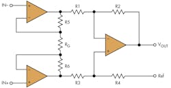
3. In the traditional three-op-amp INA, RG sets actual signal gain, but common-mode signals are only passed through the first two amplifiers at unity gain.
In this configuration, the circuit gain is set via the value of the resistor labeled RG. Looking at the input stage, consisting of the two op amps, any common-mode signal is only amplified by unity gain, regardless of the differential gain (set by RG) in the first two amplifiers. Hence, this circuitry can accommodate a wide common-mode range (limited by the headroom of the first two amplifiers), regardless of the gain. This is an advantage over the two-op-amp INA. The difference amplifier will then remove any common-mode components. Similar to the previous architectures that have been discussed, the CMR performance depends on the resistor ratio matching:
CMR = 20 log (gain * 100Rt)
where Rt = total mismatch of the resistor pairs. Because the common-mode component always sees unity gain, the CMR of the three-op-amp INA will increase proportionally with the amount of differential gain.
Several monolithic INAs are based on this circuit concept. A monolithic solution offers very well matched amplifiers, and the ability to use trimmed resistors results in good CMR and gain accuracy. More recently, monolithic INAs have improved this basic architecture. Current-mode topologies, for example, eliminate the need for precision resistor matching to achieve high CMR. In any case, a discrete solution using op amps and discrete components typically will be more costly and result in degraded performance.
INA And Op-Amp Specifications
Because op amps and INAs are related, and op amps can be used to construct INAs, there are some specifications that are common to both amps and INAs. But there are also specifications that are unique to INAs, due to the specific functionality of such a device. Two important specifications for measurement applications that are common between op amps and INAs are input bias current and input offset voltage/offset voltage drift.
Input bias current is the amount of current flow into the inputs of the amplifier that is required to bias the input transistors. The magnitude of this current can vary from microamps down to picoamps, and it greatly depends on the architecture of the amplifier-input circuitry. This parameter becomes extremely important when connecting a high-impedance sensor to an amplifier’s input. As the bias current flows through this high impedance, a voltage drop occurs across the impedance, resulting in a voltage error. Whether the circuit contains an op amp or an INA, bias current can play a critical role in the overall error budget of the circuitry.
Another important amplifier specification common to both op amps and INAs is input offset voltage. As the name implies, this specification is the amplifier’s voltage difference between the inverting and non-inverting inputs. This voltage offset depends on the topology of the amplifier, and it can range from microvolts to millivolts in magnitude. Like all electrical components, amplifiers will change behavior over temperature. This is certainly true of the amplifier’s voltage offset. The voltage offset is a source of error. As the offset drifts over temperature, this error becomes correlated to the temperature. Even a high-precision amplifier will be susceptible to temperature drift. Selecting a low-drift amplifier, such as an amplifier with a zero-drift topology, or implementing periodic system calibrations to calibrate out the offset and drift, can minimize this error source.
Due to the specialized nature of INAs, there are additional specifications that aren’t typically found in standard op-amp datasheets, including gain error and a non-linearity specification. Gain error is typically specified as a maximum percentage, and it represents the maximum deviation from the ideal gain equation for that particular amplifier. Variations in resistor values and temperature gradients among the resistor networks can all contribute to gain error.
The non-linearity specification also describes the amplifier’s gain characteristic. This specification defines the maximum variation from an ideal straight-line transfer function when comparing output versus input. For example, if an INA is configured for a gain of 10, then a dc input of 100 mV should produce 1 V at the output. If the input is taken up to 500 mV, then the output should be 5 V. These two points represent the straight-line input-to-output transfer function for the amplifier. The non-linearity specification highlights any deviation from this straight line.
Wheatstone Bridge
Since INAs are designed to provide differential gain and good rejection of common-mode signals, they are very popular for sensors (such as strain gauges) arranged in the classic Wheatstone-bridge configuration. A Wheatstone bridge for a strain-gauge application consists of four elements arranged in a diamond pattern, with each side consisting of a resistive element (either a strain gauge or a fixed resistor). An excitation voltage is then applied to the bridge, and the output voltage across the middle of the bridge is measured.
A quarter bridge consists of only one variable-resistor element—the strain gauge. A half bridge has two variable-resistor elements. A full bridge has all four elements as variable-resistor elements—in this case, strain gauges. The advantage of more strain gauges is an increase in sensitivity. All else being equal, a half-bridge configuration will have twice the sensitivity as a quarter bridge, while the full bridge will have four times the sensitivity as the quarter bridge (Fig. 4). In this example, the Wheatstone bridge is excited by a dc source. Assuming VDD is set to 5 V, this creates a dc common mode of approximately 2.5 V at the center taps of the bridge.
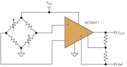
4. INAs are popular for resistive sensors in Wheatstone-bridge configurations. A quarter bridge consists of only a strain gauge, a half bridge has two variable resistors, and a full bridge has four. The more elements there are, the greater the sensitivity.
A force applied to the strain gauges will change their respective resistances, creating a small voltage differential across the center taps. This voltage change is very small relative to the common-mode voltage, typically on the order of 10 mV—hence the need to amplify this small differential voltage. An INA is ideal for this task, not only providing the needed amplification, but also rejecting the relatively high common-mode signal (and any additional noise that is common to both input signals). Keep in mind that an op amp configured as a simple gain stage will still pass the common-mode signal (at unity gain) to the output, reducing the dynamic range of the output signal.
Review
In the world of system design, the term “instrumentation” can take several meanings. Historically, the term has been used to describe the application, usually a physical phenomenon that is being measured or recorded. Hence, any op amps designed for use in such applications became known as INAs. Adding to the confusion is the fact that actual INAs can be constructed using op amps.
In reality, op amps and INAs are very different devices, designed to perform different functions. INAs can be seen as specialized amplifiers, used specifically for their differential-gain and CMR capabilities. Circuits implementing traditional op amps can be created to perform these same functions. But in most cases, a monolithic INA will provide a substantially higher level of performance and reliability.

About the Author
Kevin Tretter
Principal Product Marketing Engineer
Kevin Tretter is a principal product marketing engineer with Microchip’s Analog and Interface Products Division in Chandler, Ariz. He is responsible for tactical marketing support for Microchip’s analog and interface products in the Eastern and South Central United States, as well as strategic marketing of operational amplifiers, instrumentation amplifiers, comparators, and programmable gain amplifiers. Prior to joining Microchip in 2004, he spent five years as an audio/industrial converter applications engineer with Cirrus Logic in Austin, Texas. He earned his bachelor of science degree in electrical engineering from the Rose-Hulman Institute of Technology, Terre Haute, Ind., in 1999 and his master of business administration degree from Saint Edwards University, Austin, Texas, in 2006.
Comment About the Article
To join the conversation, and become an exclusive member of Electronic Design, create an account today!

Leaders relevant to this article: