fig_1

Examining Semiconductor Wafer Production

March 14, 2024
Taking a look at wafer production best-practices and how to leverage capacitance-based inspection systems.

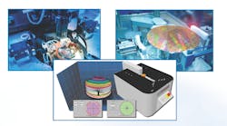
Semiconductor wafers are cut from cylindrical silicon crystals, or ingots and the flatness of these disc-shaped wafers must be tightly controlled. These tight tolerances are needed to ensure that the entire wafer surface is suitable for integrated circuit (IC) production. This process includes steps like lapping and polishing, thin film deposition, and lithography.
 
This ebook delves into the semiconductor wafer production and why out-of-spec wafers are costly mistakes that can be avoided. It is even possible to reprocess a wafer that does not meet specifications. Of course, this means having an efficient and effective inspection process.
This article explains why disc geometry matters at each step in wafer processing – and what can go wrong.


Sponsored by
Sponsored

What is Electrical Impedance?

Having trouble understanding electrical impedance? Dont worry; youre not alone. Lets get practical.

Top 10 Design for Manufacturing Mistakes Every PCB Manufacturer Hates

Ever wonder what kind of Design for Manufacturing (DFM) mistakes you can make that will drive your PCB manufacturer absolutely crazy? Learn about the top 10 DFM mistakes now, ...

Next Generation RADAR

Aerospace and Defense applications conform to the tightest standards. ADI provides you with the confidence and support to ensure your design is a success.

What is a Field Effect Transistor (FET)?

Ever wonder what a Field Effect Transistor (FET) is? Give this article a read for everything you need to know about the device.