This article is part of the TechXchange: Distinguishing Discretes.
What you’ll learn:
- Why silk is being used for bio-compatible transistors.
- How the silk is transformed to develop the transistor function.
- The two types of operation provided by the silk-based transistor.
Silicon and other semiconductor materials such as gallium nitride (GaN) or silicon carbide (SiC) have well-known incompatibilities with living tissue, and considerable work is being done to resolve that problem. Now, a team at Tufts University has devised a different approach. They’re replacing traditional materials with biological silk and its derivatives to create biocompatible transistors.
Their fundamental electronic components are partly biological and will respond directly to the environment and change like living tissue. The silk fibroin—the structural protein of silk fibers—can be precisely deposited onto surfaces and easily modified with other chemical and biological molecules to change its properties.
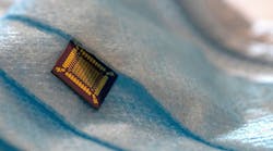
Their modified silk can pick up and detect a wide range of components from the body or environment. The team’s first demonstration of a prototype device used hybrid transistors with silk fibroin to make a highly sensitive and ultra-fast breath sensor, detecting changes in humidity.
This is not their first silk-related project. Prior to this development, the Tufts Silklab (yes, that’s a real place), led by Fiorenzo Omenetto, the Frank C. Doble Professor of engineering, had already used fibroin to make bioactive inks for fabrics that can detect changes in the environment or on the body. They also created sensing tattoos with fibroin that can be placed under the skin or on the teeth to monitor health and diet, as well as sensors that can be printed on any surface to detect pathogens like the virus responsible for COVID-19.
How Does the Bio-Hybrid Silk Transistor Work?
In a biological-hybrid transistor, a silk layer is used as the insulator, and when it absorbs moisture, it acts like a gel carrying whatever ions (electrically charged molecules) are contained within. The gate triggers the on-state by rearranging ions in the silk gel. By changing the ionic composition in the silk, the transistor operation changes, allowing it to be triggered by any gate value between zero and one.
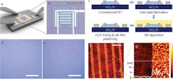
The technical challenge in creating these biological-hybrid transistors was to achieve silk processing at the nanoscale level, down to 10 nm (Fig. 1).
1. Silk‐FET architecture and fabrication: (a) Graphic representation of an indium-gallium-zinc oxide (IGZO) silk‐FET with lateral gate electrode interfaced with an ultra-thin silk layer. (b) A microscopy image of the device. (c) Fabrication schematics. (d,e) Microscopy images of the ultra-thin silk films patterned in squares (d) and stripes (e) on a Si/SiO2 substrate (scale bars: 50 µm). (f,g) Atomic force microscopy images of stripe‐patterned silk films (scale bar: 10 µm) and the profile (inset of (g)) .
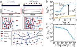
The devices offer two distinct modes of operation—either traditional field-effect or electrolyte-gated—enabled by the precisely controlled thickness, morphology, and biochemistry of the integrated silk layers. The different operational modes are selectively accessed by dynamically modulating the free-water content within the nanoscale protein layer from the vapor phase (Fig. 2).
2. Silk‐FET operating mechanism: (a) Representation of a planar capacitor with electrodes in direct contact with an ultra-thin silk layer in either dry or humid conditions (left and right, respectively) displaying the expected lateral profiles of the potential (black) and of the electric field (red) across the insulating layer in the two cases. (b) Transfer characteristic curve of a silk‐FET in either dry or humid conditions. (c) Specific gate capacitance measurement performed in humid conditions.
The team demonstrated that at these length scales, the absorption and transport of water molecules in the biomaterial, which can be introduced from either direct vapor streams or from changes in environmental humidity, leads to the dynamic and reversible formation of electrical double layers (EDLs) at the semiconductor/silk and at the metal/silk interfaces.
They exploited this formation in inorganic thin-film field-effect transistors (silk-FETs) that can readily switch from traditional field-effect mode to electrolyte-gated operation. This humidity-controlled reconfigurability was demonstrated within a compact and highly sensitive breath sensor (Fig. 3).
3. Silk‐FET operating mechanism: (a) Representation of a planar capacitor with electrodes in direct contact with an ultra-thin silk layer in either dry or humid conditions (left and right, respectively) displaying the expected lateral profiles of the potential (black) and of the electric field (red) across the insulating layer in the two cases. (b) Transfer characteristic curve of a silk‐FET in either dry or humid conditions. (c) Specific gate capacitance measurement performed in humid conditions.
The work is detailed in their short paper published in Advanced Materials with the non-obvious title “Bimodal Gating Mechanism in Hybrid Thin-Film Transistors Based on Dynamically Reconfigurable Nanoscale Biopolymer Interfaces.” There’s also a brief Supplemental Materials file available.
Read more articles in the TechXchange: Distinguishing Discretes.


