Although microcontrollers generally run at low voltages, such as 3.3 V, they often need to control loads running at higher voltages like 12 V. If switching the low side isn’t an option, the microcontroller needs a way to control a high-side switch from its low-voltage output.
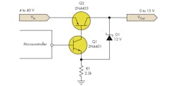
The circuit in the figure provides a simple solution. Besides using few components, it provides overvoltage protection as a bonus. As long as the input voltage stays below approximately 15 V, the output voltage will equal the input voltage (minus the tiny VCE drop across transistor Q2).
Once the input voltage exceeds that limit, however, the circuit begins acting as a low-dropout regulator (LDO), limiting the output voltage to 15 V. This feature is useful if the input voltage occasionally exceeds the rated load voltage, but the load switch needs to remain efficient otherwise.
Transistor Q1 and resistor R1 form a current sink. The microcontroller’s output voltage (VOH) and Q1’s base-emitter drop (VBE) create a stable voltage across the resistor, producing a current of (VOH – VBE)/R1, or about 1.2 mA for a 3.3-V microcontroller. Most of this current flows through Q2’s base, which controls the load. This current drops to zero when the microcontroller output goes low, switching the load off.
Zener diode D1 provides an alternative path for R1’s current. If the diode’s breakdown current is VZ, it will begin to conduct when the output voltage exceeds VZ + VOH – VBE, or about 14.6 V for a 12-V diode and a 3.3-V microcontroller. Since the voltage across R1 is constant, the diode effectively “steals” current from the base of Q2, reducing the amount of current flowing into the load. This negative feedback causes the circuit to act like a voltage regulator.
To apply this circuit to your application, adjust R1 so Q2’s base current equals the maximum load current (IMAX) divided by Q2’s gain (b), or R1 = b×(VOH – VBE)/ IMAX. Be sure to select a transistor for Q2 that can dissipate the heat generated during an overvoltage event.
There is no straightforward way to calculate the exact output voltage, so the quickest approach is to try a few Zener diode voltages and pick the one that works. A good starting point is to pick Zener voltage VZ to equal to the desired output voltage minus the microcontroller voltage. This is just an overvoltage protector, so great accuracy should not be necessary.
If the overvoltage protection isn’t important, simply remove the Zener diode. The resulting load switch uses only three components and retains the advantage of driving Q2’s base with an actual current source. Even if the input voltage changes, Q2’s base current remains constant.
The microcontroller turns the load off by controlling a high-side switch formed by Q1 and Q2. The current-sink action of Q1 controls the load voltage.

