This file type includes high-resolution graphics and schematics when applicable.
Günther Schindler, CEO, Schindler
It’s costly and time-consuming to determine the causes of hotspots on circuit boards, and to attempt to arrive at a “well-tempered” board through multiple iterations once a prototype is approved. A thermal simulation would help to reduce the effort and expense.
Up to now, though, such simulation has primarily been the task of specialized physicists and part of the mechanical evaluation of a PCB’s design. However, it’s possible to solve thermal problems in the development and layout stage with a simulation tool known as PCB-Investigator Physics (PCBi Physics).
PCBi Physics is an extension of EasyLogix PCB-Investigator, a CAD/CAM software solution from Schindler & Schill GmbH. This CAD/CAM software is primarily designed to simplify review processes connected with the development of electronic assemblies and make them more efficient with the help of comprehensive tools for import, export, and visualization.
The software reads layout data in a variety of formats (ODB++, DXF, GenCad 1.4, Gerber 274x, etc.), making it independent of the systems already in use. Its functionality isn’t limited to conducting paths and surfaces; it also includes complete information on the layout’s components and networks. All layers and data objects, such as components, pins, networks, and copper elements, can easily be accessed using the review function.
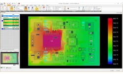
This holistic view also offers a new approach to heat management. The PCBi Physics extension enables developers to discover problematic heat build-up in future products at a very early stage of development and avoid it in a targeted manner. The thermal simulation is embedded in the CAD/CAM software and can be accessed at the push of a button without the developer having to bring in an expert (Fig. 1).
1. This thermoscan is the result of a simulation run using PCB-Investigator.
Tried and prove technology
TRM (Thermal Risk Management), produced by ADAM Research, is the engine under the hood of PCBi Physics. Both TRM and the tool from EasyLogix are able to integrate multilayer boards, surface-mount-device (SMD) heat sources, embedded components, pins, inlays, power rails, through-holes, blind vias, and buried vias.
Comparisons show that simulations differ from infrared thermographs of finished boards by only ±10% or less in normal cases. The graphical representation of the results corresponds to that of a thermograph and is even more informative in certain cases.
For example, hotspots in internal layers cannot be reliably detected on the surface via thermography, but PCBi Physics simulations are able to reveal them. PCBi Physics uses the information available in the CAD/CAM software to depict temperature increases caused by dissipation from components and currents. The current density, for example, in copper bottlenecks or holes, is factored in at one go, as are voltage drops and line resistance between pins on every layer.
How Does the Heat Distribute Itself?
The temperature of the conducting paths and components characterizes the thermal equilibrium between the heat dissipation of the components and currents on the one hand, and the cooling caused by the environment on the other. Particular consideration must be given to the heat splay in the layers and in FR4 in order to arrive at a meaningful conclusion in this area.
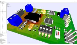
2. In this 3D view of a fully mounted board, you can see how heat accumulates under the large black component.
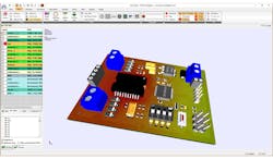
This means that placement, layout, and holes must be factored in from both a geometrical and physical standpoint. And the software does exactly that for every layer, every conducting path, and every hole (Figs. 2 and 3).
3. Shown is a simulation of how heat would be distributed if the board in Figure 2 had four layers. The prognosis is that additional copper layers ensure homogeneous behavior and would offer a solution to the hotspot.
2D vs. 3D
Standard software for computational fluid-dynamics simulation, such as Autodesk CFD, FloTHERM, 6SigmaET, ANSYS Icepak, or COMSOL Multiphysics, is a powerful tool for predicting the temperature behavior of PCBs when used by experts. The problem is that all of these programs are based on 3D models or involve flow calculations that require additional effort, considerable memory resources, and long computation times.
Not only does this entail additional effort and expense, but it also makes it difficult to integrate the simulation into the development process at an early stage. Circuit-board layouts are designed in 2D, yet the thermodynamic simulators don’t offer a 2D editor. By contrast, PCBi Physics is based on 2D models, but runs 3D simulations. In addition, it offers a full-shape modeler mode that models the PCB geometry of each layer and the positions of every through-hole for a precise voltage simulation.
Because PCBi Physics always takes the current flow into account, it allows users to keep an eye out for EMC problems, for example. To put it simply, a longer conducting path may be welcome from a purely thermal standpoint as a way of dissipating heat, but it may also have the undesirable side effect of acting as an antenna.
Virtual Thermal Image
The temperature computations factor in contributions from electric heating and heat input from the components and calculate heat propagation in each layer, hole, and prepreg. Thermal hotspots, critical line resistances, and excessive voltage drops can be geometrically pinpointed with great accuracy. As a result, the user obtains thermal images (typically as precise as the thickness of a 0.2-mm pencil lead or better) for each copper and prepreg level, as well as detailed maps of current densities, potentials, voltage drops, temperature-dependent material properties, and local heat output.
There are often several factors that influence temperature. The simulation makes it easy to distinguish quickly between important and unimportant influences. When using the editor function, the layout or layer structure of a PCB can be optimized with just a few clicks (2D changes made directly in ODB++).
Optimizing at an Early Stage
The plug-in for PCB-Investigator offers several advantages. For instance, the integration of a fully developed, specialized solution (ADAM Research TRM) allows users to run simulations at the push of a button, without training in numerical methods. Direct editability makes it possible to quickly eliminate potential hotspots. As a result, thermal simulations can also be used to monitor iterative design cycles when optimization is the goal.
However, avoiding heat build-up at an early stage is just one objective. The simulation results also provide information on whether temperature specifications could still be met with thinner copper, fewer layers, or without heat sinks.
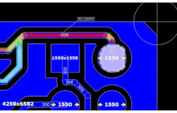
4. PCB-Investigator Physics enables users to predict thermal problems and helps with optimization. Here, a conducting path 300 µm in width and a specified current density of 41.7 A/mm². By conducting a heat simulation based on this information, the user could determine whether the conducting paths would make do with less copper.
If, for example, the design of a PCB calls for 105 µ of copper and the simulation shows that it only heats up slightly, the designer could simply change the thickness to 70 µ in the simulation and then recalculate. The simulation therefore indicates potential for savings, both with regard to space requirements and the use of raw materials.
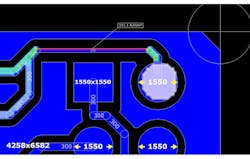
It can also influence another cost factor—the number of holes for thermal vias. The simulation enables users to recognize ineffective holes and either eliminate them or find a better place for them (Figs. 4 and 5).
5. This conducting path measures 150 µm wide, which results in a current density of 111.1 A/mm². Again, the PCB-Investigator Physics tool could help determine thermal problems, and offer ways to optimize the situation.
Conclusion
Miniaturization is an ongoing topic in electronics development, and critical temperature development is one of its limiting factors. When developers are able to conduct thermal simulations by themselves at an early stage without special effort, this generates potential for optimization and reduces the number of necessary prototypes and measurements.
