Download this article in PDF format.
Every verification engineer today knows about hardware emulation and its capabilities. Some may know it’s a technology employed since the 1980s. However, not everyone knows the story of emulation’s winding path from a tool relegated to the dusty backrooms to widespread adoption, or the players involved.
Follow me as we take a stroll through the hardware emulation archives for its remarkable journey.
What Started It All
In the second part of the 1980s, hardware emulation sprang from the invention of the field-programmable gate array (FPGA). By building an array of interconnected FPGAs configured to “emulate” the behavior of a design before silicon, it was possible to verify the design at speeds unapproachable by any software-based simulation algorithm. The high-speed led to testing the design-under-test (DUT) with real input-output traffic via a physical target system, where ultimately the chip would reside once released by the foundry. The DUT combined with the target system setup is called in-circuit emulation or ICE.
FPGA-based emulators were time-consuming to deploy and rather difficult to use. In fact, the industry devised the expression “time-to-emulation” (TTE) to measure the time required to bring up the DUT for emulation and start to emulate it. Measured in several months, the TTE often exceeded the time it took for the foundry to release first silicon.
It was apparent from the very beginning that the FPGA-based emulation architecture was severely deficient. What was even more troublesome was that it could not be re-engineered to eliminate its inherent drawbacks. A long setup time, exceedingly slow compilation speed, and poor visibility into the DUT were hallmarks of the off-the-shelf FPGA-based emulator.
By the middle of the 1990s, a few innovative startups proposed new technologies to overcome the drawbacks. They believed that only custom-made silicon designed for emulation held the promise to remove the pitfalls of the old class of emulators.
New Design Approaches
From the start, all of the initiatives were based on custom reprogrammable devices deployed in two rather different emulation architectures.
One made use of a custom FPGA designed to provide 100% native internal visibility of the DUT without compiling probes. The unique architecture also offered easier setup time and significantly faster compilation speed.
The other architecture took a radically different approach, achieving the same objectives: 100% native visibility into the DUT, easier setup time, and very fast compilation speed. It was called a custom-processor-based emulator.
Twenty years later, these design approaches are the architectures for today’s hardware emulation, though far, far superior to the early days.
Approach 1: Custom FPGA-Based Emulator
In the early 1990s, a French startup, Meta Systems, conceived a custom FPGA designed specifically for emulation. The chip encompassed an entire emulator; hence, it was called emulator-on-chip, and included configurable elements, a local interconnect matrix, a set of embedded multi-port memories, I/O channels, DUT debug circuitry, and clock generators.
The custom FPGA shared some similarities with the commercial FPGA, but possessed unique capabilities, including two innovations, each offering distinctive benefits:
- A creative interconnection network of programmable elements
- Integrated DUT debugging capabilities
Internal Interconnection Network of Programmable Elements
The interconnection network of the programmable elements included two hierarchical layers: a lower layer at the lookup-table (LUT) level, and a higher layer encompassing large blocks of LUT clusters, called tiles.
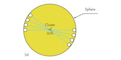
A spatial analogy can describe the layout. Assuming that all LUTs would be located on the surface of a sphere, and the interconnection of any two LUTs should cross the center of the sphere, the length of the interconnecting wire would always be the same. This would happen regardless of where the two LUTs would be located.
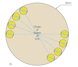
The 3D analogy could be extended to the higher hierarchical level, where clusters of LUTs may be distributed on the surface of a larger sphere and interconnected with the same scheme (Fig. 1).
1. Any two LUTs on the surface of a sphere, as pictured here, must cross the sphere’s center when interconnecting; the length of wire connecting the two is always the same, no matter where they are located (a). A LUT cluster can be distributed on a larger sphere and interconnected with the same scheme (b).
The layout is a fractal graph where the same pattern is repeated, moving from the outside to the inside or from the inside to the outside.
The higher layer interconnected the tiles with a matrix of tiny crossbars. It’s somewhat analogous to a network-on-chip (NoC) architecture, which set this structure apart from the traditional mesh interconnection network for predictable, fast, and congestion-free routing.
Furthermore, clock trees were wired on dedicated paths independent from and shorter than data paths, guaranteeing predictable and repeatable timing as well as preventing timing violations. Unpredictable timing and hold-timing violations were major drawbacks of emulators based on commercial FPGAs.
The multi-layer interconnection network traded off high capacity for fast and congestion-free FPGA place-and-route (P&R). It was possible to P&R one custom FPGA in about five minutes, which was much different than the several hours required by off-the-shelf FPGAs.
Integrated Design Debugging Capabilities
The second innovation concerned integrated DUT debugging capabilities.
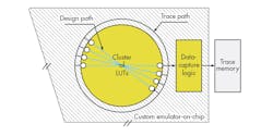
Total visibility was achieved by connecting all LUTs and embedded-memory outputs to on-chip signal probing circuitry, avoiding the need to route them at compilation time. In turn, the probing circuitry directed on-the-fly captured data to a bank of fast memory chips, coupled to custom emulator-on-chip devices mounted on the emulation board. The dedicated routing resources did not make use of the internal LUT interconnection network and increased the efficiency of the reconfigurable hardware (Fig. 2).
2. The custom emulator-on-chip includes dedicated logic for full visibility and fast debugging without requiring the compilation of probes.
Design debug capabilities were augmented by an integrated triggering mechanism and a built-in logic analyzer with a graphical path browser that accelerated the identification of difficult-to-find bugs. The emulator-on-chip enabled triggering on registers by default, force-n-release, memory/register peek-and-poke, and save-n-restore.
An often-overlooked side benefit of the custom-FPGA approach was that the supplier owned the technology and therefore was in control of its destiny. For example, it could optimize and customize the P&R software and manage manufacturing of the chip. The supplier of emulators based on a commercial FPGA was at the mercy of FPGA vendors.
In 1996, Mentor Graphics (now Mentor, a Siemens business) acquired Meta Systems, and the emulator-on-chip architecture became a fundamental emulation technology at Mentor. After the acquisition of IKOS Systems in 2002, Mentor enhanced the emulator-on-chip architecture by adding the Virtual Wire technology devised by Virtual Machine Works. The Virtual Wire technology consisted of synchronous multiplexing of the FPGA I/O pins to transmit several I/O signals on a single pin under the control of a timing scheduling process. The new emulation platform was called Veloce. Over time, Mentor introduced three generations of Veloce emulators.
Approach 2: Custom Processor-Based Emulator
A second innovation initially was devised by IBM, a processor-based architecture for acceleration that the company created for internal use only. IBM never launched a commercial version.
Conceptually, a processor-based emulator is made up of a vast array of simple Boolean solvers or processors that gave the emulator type its name. Typically, the vast array is made up of relatively simple 4-input arithmetic logic units (ALUs), possibly reaching into the millions in expanded configurations. The DUT model is compiled into a data structure stored in memory, and the processors are tasked with evaluating all logic (Boolean) functions in the DUT in a timely order controlled by a sequencer.
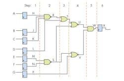
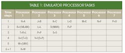
The principle of the operation is exemplified in Figure 3 and Table 1, using a simplified approach.
3. Logic functions in the DUT are controlled by a sequencer in a timely order.
An emulator’s processors are tasked with evaluating functions in the DUT in a time order controlled by a sequencer.
All operations are scheduled in time steps and assigned to the processors according to a set of rules to preserve the DUT’s functional integrity.
An emulation cycle runs all of the processor steps for a complete design execution. Large designs typically require hundreds of steps. The more operations carried out in each step, the faster the emulation speed.
During each time step, each ALU executes its inputs generated by processing of the upstream ALUs, memory contents, and design primary inputs. The more processors installed in the emulator, the more parallelism can be achieved with the benefit of faster execution time.
The compiler must partition the DUT among the processors and schedule individual Boolean operations in time steps, optimizing the processor scheduling for any given configuration of the emulator to maximize speed and capacity. It also considers several additional issues, such as tri-state bus modeling, memory modeling, debug probing, triggering, and other factors.
The compiler doesn’t have to deal with the internal timing of the commercial FPGA-based emulators, one of the most critical issues in these emulators. Controlling timing in an array of FPGAs is hard, unpredictable, and a path to failure, unless attention and engineering talent is involved in designing the compiler.
In a processor-based emulator, no P&R is involved. Thus, compilation is much faster and requires fewer resources than off-the-shelf FPGA-based emulators.
Unlike the hard limit in design capacity of the FPGA-based emulators (when all FPGA resources are used; no room for larger designs is available), the processor-based scheme allows for a somewhat soft limit in design capacity. A user could slightly exceed the maximum capacity specified by the vendor, maybe by as much as 10%, at the expense of a drop in performance that may be significant.
Advantages of the processor-based emulator came at the cost of higher power consumption than FPGA-based emulators. All of those tiny processors are actively running all of the time and consume plenty of energy. In fact, the system requires fluid-cooling, removing flexibility in placing and adding cost for A/C.
In 1996, IBM OEM’d its technology to Quickturn, the leader in hardware emulation at the time. One year later, Quickturn launched the first commercial version of a processor-based emulator under the name CoBALT (Concurrent Broadcast Array Logic Technology), as an alternative to Quickturn’s standard FPGA-based emulators.
Then in 1998, Cadence purchased Quickturn, and ultimately discontinued the FPGA-based approach. The company claimed it was inferior to the processor-based architecture in three main areas: slow setup-time and compilation time; poor debugging capabilities; and a significant drop in execution speed as design size increases.
IBM wasn’t the only company experimenting with processor-based architectures. Another company that undertook the same route was a startup by the name Arkos. While still in stealth mode, it was acquired by Synopsys in 1996. Soon after the acquisition, Synopsys introduced its processor-based emulator. It turned out to be a flop and Synopsys quickly sold the technology and patents to Quickturn.
Other Hardware Emulation Approaches
While the two classes of emulation architectures based on custom silicon got most of the attention, the commercial FPGA-based method did not fade away. Two notable examples are worth mentioning. In one instance, FPGAs were used in a novel approach by a startup named Axis. In the other, a company named Emulation Verification Engineering (EVE) adopted the conventional approach driven by new generations of large-capacity FPGAs that promised to alleviate the I/O-limited bandwidth of the old generation of FPGAs.
Axis
In 1998, a startup named Axis, devised an interesting architecture based on a ReConfigurable Computing (RCC) technology. While no technical details were ever made public, its verification system essentially mapped a verification algorithm onto an array of commercial FPGAs and executed the DUT-compiled code. It was first launched as an accelerator under the name of Xcite, and later, significantly enhanced in execution speed as an emulator named Xtreme.
Axis was acquired by Verisity in 2003. In 2005, Cadence purchased Verisity, and soon after permanently shelved the Axis verification technology.
EVE
In 2002, EVE introduced an emulator on a PCI card based on Virtex-6000/8000, the largest Xilinx FPGAs of the time and called it ZeBu-ZV. In the following decade, EVE launched five generations of ZeBu in two product lines. It continued with the PCI-card approach, upgrading the Xilinx FPGA with newer generations, and launched an emulator in a box for larger capacity, upgrading it with newer generations of FPGAs. Table 2 summarizes the ZeBu family.
EVE’s ZeBu emulator family used the largest available Xilinx FPGAs.
ZeBu was a hybrid between the traditional emulator and an FPGA prototyping system. In the box configuration, it had higher design capacity than an FPGA prototype, but less than the leading emulators. It offered higher speed of execution than leading emulators, but less than any FPGA prototype. Setup time and compilation speed were better than in the FPGA prototype, but far worse than in the leading emulators. Design debugging was better than in FPGA prototypes, but inferior to the state-of-the-art emulators. It was most effective for system validation and hardware/software integration.
Synopsys acquired EVE in 2012, and to date continues the development of the ZeBu-Server family with newer Xilinx Virtex FPGAs.
Conclusion
By the beginning of the second decade of the new millennium, industry consolidation left three emulation players: Mentor, Cadence, and Synopsys. Each uses its unique architecture based on one of three approaches listed in Table 3.
These three emulation providers each use different approaches to their technology.
All three vendors continue to push the technological envelope of their own emulation platforms, and compete in the market with new generations still based on three different architectures. Of course, many new advances, features, and capabilities make emulation a foundational tool in almost all chip design verification flows.
Dr. Lauro Rizzatti is a verification consultant and industry expert on hardware emulation. Previously, Dr. Rizzatti held positions in management, product marketing, technical marketing and engineering.
