How New DAC Technologies are Changing Signal Generation For Test
Download this article in PDF format.
Digital-to-analog converters (DACs) have been widely used since the 1980s in arbitrary function generators (AFGs) and arbitrary waveform generators (AWGs) to produce signals for verification, characterization, and stress/margin testing. However, advances in DAC technologies and techniques enabled them to directly generate highly detailed RF and electronic-warfare (EW) signals or the complex pulse trains used in advanced research, making them very suitable for high-end applications such as quantum computing.
These high-end applications include wideband RF systems, validation of high-speed silicon, coherent optical research, and leading-edge research in electronics, physics, and chemistry. If a waveform can be defined or captured, chances are a modern AWG with high sample rates can generate the signals of interest.
For some applications like radar, EW, and advanced research, there’s more to the story than top-line sample-rate performance. Factors such as price per channel, signal fidelity, and scalability have become increasingly important. High-performance equipment that can meet speed and bandwidth requirements is expensive, particularly for projects that require multiple synchronized channels.
Signal Processing Behind DACs’ Advances
Designing a DAC with both a high number of bits and a high sample rate with good dynamic range has proven to be a difficult undertaking. While this has been a hindrance in the past, DAC technology is now far enough along that it’s possible to directly generate high-frequency signals with high fidelity directly out of the DACs. There are still some limitations and times when an upconverter or mixer may still be needed, but modern DACs can cover signal requirements for the ISM band and LTE 5G up to 5 GHz.
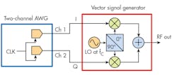
1. I and Q signals for RF and microwave applications are generated using a two-channel arbitrary waveform generator supplying a microwave vector signal generator. However, this technique has a major disadvantage of degradation in signal-modulation quality.
Driven in part by the demand for lower-cost and smaller-size devices for telecommunication and military systems, DACs are also now starting to incorporate signal processing and modulation in addition to signal-generation functionalities. In the past, a separate system handled the signal processing and created the waveform, and the digital information was fed into the DAC. Now, more advanced high-speed DACs have signal-processing blocks built right into them.
The more useful of these digital-signal-processing blocks include complex (or I-Q) modulation, numerically controlled oscillators (NCOs), and conditioning functionalities such as finite-input-response (FIR) filters and digital interpolation. This enables direct generation of complex RF signals in an efficient, compact, and ultimately more affordable way. This in turn is leading to a new generation of AWGs that are well-suited to many more advanced and complex RF and advanced research applications, including quantum computing.
Microwave Signal Generation
To fully appreciate why these advances in DAC technology are so significant, it’s helpful look at the challenges of generating complex microwave signals. A common method to generate complex signals is to modulate a carrier signal with a frequency generated by a local oscillator (LO) using a vector modulator, essentially a hardware implementation of the following trigonometric identity:
This formula can conveniently be implemented in hardware by noting that sin(ωct) = cos(ωct + π/2), which implies that by shifting the phase of the carrier signal by 90 degrees, the sine and cosine terms to left-hand side of the above equation can be produced from a single sinusoidal source. The I and Q terms are the in-phase and quadrature baseband signals, respectively. These terms can set the amplitude and phase of the carrier signal to any arbitrary value, which allows for the implementation of any type of modulation.
For RF and microwave applications, generation of I and Q signals are typically done using AWGs that, at their core, contain multiple synchronized DACs. Figure 1 shows a two-channel AWG supplying the I and Q signals to a vector signal generator (VSG).
A major disadvantage to this technique is the degradation in signal-modulation quality due to both phase and amplitude imbalances in the I and Q signals, as well as residual leakage from the local oscillator (LO). This is due to vector modulator hardware limitations that can, to some extent, be compensated for and corrected through a series of calibration operations. Because of the need for more equipment, cost and complexity can be significant problems for large-scale, multichannel RF systems.
For example, in a superconducting quantum-bit (qubit) controller system, where the frequency of the signals used for excitation of qubit resonators need fine-tuning, each RF channel requires a VSG with an independent tunable LO and two channels of an AWG. In addition, LO leakage limits the dynamic range in pulsed signal applications that need a stable, high on-to-off ratio.
High-Speed DACs with Complex Modulators
The latest DACs overcome many of the problems with generating complex microwave signals by integrating more functionality into a single chip. Looking at a simplified block diagram of a high-speed 16-bit DAC being used in next-generation AWGs, the design incorporates a digital complex modulator and multi-rate interpolation (Fig. 2).
2. This simplified block diagram of the DAC in a more recent generation AWG shows the level of functional integration that helps overcome many of the problems of older generations.
The complex modulator is a digital implementation of a VSG. The NCO acts as the local oscillator providing the carrier signal. The user-defined I and Q baseband signals are digitally streamed into the DAC from an off-chip memory. The output of this modulator is a digital waveform applied to the DAC core. The NCO’s frequency is controlled using a dedicated on-chip register that can be independently programmed, allowing for the carrier frequency to be tuned without recalculating or reloading of the I-Q waveforms.
Interpolation in the digital data path is used to generate waveform data, which is supplied to the DAC at lower sample rates to reduce memory requirements. Two independent interpolation blocks are included—a baseband block with selectable factors from 2x to 16x, and a block associated with the double-data-rate (DDR) clocking feature.
When DDR is off, data is converted on only one of the clock edges and the interpolation mode is set to x1. When DDR mode is used, data is 2x interpolated and converted on both edges of the clock signal. While in DDR mode, the NCO’s sample rate also doubles. As a result, at the maximum clock frequency of 5 GHz, the NCO and the DAC core are running at a sample rate of 10 Gsamples/s and carrier frequencies up to 5 GHz in the first Nyquist band can be synthesized.
With a reconstruction filter at the output of the AWG, analog signals with complex modulation can be directly generated up to nearly 5 GHz. Signals at higher frequencies are also possible using higher-order Nyquist bands.
Direct Signal Generation
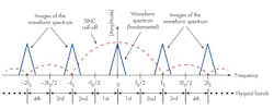
The magnitude of the complex output spectrum of a DAC generating an arbitrary waveform is shown (Fig. 3). At every half-sample rate interval, there’s an image of the waveform spectrum. These intervals are referred to as the Nyquist bands and the spectrum is inverted in even-order bands.
3. Illustrating the magnitude of a DAC’s complex output spectrum, the images can be used to directly generate signals at higher frequencies within the limitations imposed by the SINC roll-off in amplitude.
By applying the appropriate analog filter and amplifier to the output of the DAC, these images can be used to directly generate signals at higher frequencies, within the limitations imposed by the SINC roll-off in amplitude. Other considerations for direct signal generation in the higher-order Nyquist bands include the noise floor of the DAC and spurious products that could limit dynamic range.
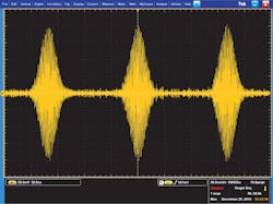
Figure 4 shows the time-domain measurement of the 2nd Nyquist image of a 20-ns Gaussian pulse created using complex modulation with the sine of the Q baseband waveform inverted. The AWG clock was set to 3.584 GHz, the DDR mode was enabled, and the baseband waveform data interpolated by 2x, which sets the sample rate of the I and Q waveforms to 1.792 Gsamples/s and the final sample rate to 7.168 Gsamples/s. The NCO frequency was set to 2.168 GHz, which produced the 2nd Nyquist image centered at 5GHz.
4. Shown is the time-domain measurement of a 20-ns-wide Gaussian pulse with carrier frequency of 5 GHz in the 2nd Nyquist band.
For this measurement, no external filter or amplifiers were used. However, the acquired waveform was post-processed by applying a 350-MHz-wide digital FIR bandpass filter centered at 5 GHz to remove the fundamental signal.
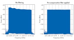
The amplitude and phase distortion due to the composite frequency response of the AWG and external components can be compensated by applying a FIR filter to the I and Q waveforms in the digital domain. The effect of applying such a filter to a multi-tone waveform in the 2nd Nyquist band centered at 5 GHz is shown (Fig. 5). This waveform was also created using the complex modulator with the same AWG setting as for the Gaussian pulse.
5. Here’s the power-spectrum measurement of a multi-tone waveform in the 2nd Nyquist band comprising 361 tones with 1-MHz spacing from 4.82 GHz to 5.18 GHz without filtering (left) and with a digital pre-compensation filter applied (right).
Superheterodyne Upconversion
Even with the improved performance and lower noise floor of the latest DACs, there will be cases where the desired frequency is too high to effectively use the higher-order Nyquist bands, and with good dynamic range. In these cases, a superheterodyne upconversion scheme incorporating the NCO and an external mixer is a useful way to extend the AWG’s output frequency coverage.
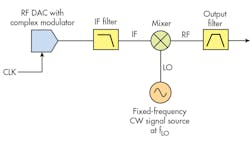
Superheterodyne upconversion is performed in two stages, where the signal is first upconverted to an intermediate frequency (IF) and, after filtering out the undesired spectral components, the IF spectrum is upconverted again to a higher RF band (Fig. 6).
6. This superheterodyne-upconversion setup uses an RF DAC with a digital complex modulator and an external mixer with a fixed-frequency LO.
The AWG’s DAC digitally upconverts the signal to an IF band using its internal digital complex modulator and the NCO, followed by an external mixer driven by a fixed-frequency local oscillator that produces the final output spectrum. In this setup, either a low-pass or a bandpass filter may be needed at the output of the AWG to remove signal spectrum images before applying it to the IF port of the mixer.
While this is a somewhat more complex setup than what’s needed for lower frequencies, having a fixed LO comes at significantly lower cost for complex microwave signal generation, relative to the traditional VSGs that use IQ modulators and analog synthesizers as the LO. Furthermore, only one channel of an AWG is needed to generate both the I and Q baseband signals. A VSG, on the other hand, requires two channels of an AWG: one for the I waveforms and another for the Q waveforms.
Also in contrast to VSG, the LO leakage is out-of-band from the main signal spectrum and can be filtered out. This is extremely advantageous when a very high on-to-off ratio is desired for pulsed signals. Also, since the modulation is done in the digital domain, the quadrature relationship between the I and Q waveforms over the entire signal bandwidth is preserved. As a result, there’s no need for calibration to correct the I-Q imbalance. Distortion due to the frequency response of the analog path can be compensated for by applying pre-compensating FIR filters to the I and Q waveforms in the digital domain.
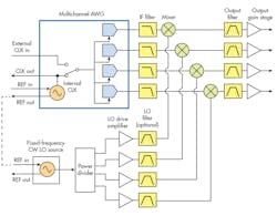
7. A shared LO source is split four ways in this multichannel superheterodyne-upconversion configuration.
Superheterodyne upconversion can efficiently be extended to a larger number of AWG channels by sharing the LO source (Fig. 7). The image shows a 4-channel AWG where a single LO source is split four ways using a power divider that drives the mixers.
Conclusion
The availability of new high-performance DACs that offer a mix of speed and resolution within a fully integrated product package are enabling the development of AWGs that can directly generate highly detailed RF/EW signals or the complex pulse trains used in advanced research. Featuring 16-bit resolution, these instruments can provide a 10-Gsample/s rate and as many as eight independent channels with better than 10-ps channel-to-channel skew.
