Combat Semiconductor Noise with These Isolation Methods
This article is part of the TechXchange: Delving into EMI, EMC and Noise.
Members can download this article in PDF format.
What you'll learn:
- What is high-voltage CMOS isolation?
- A look at ohmic contact substrates.
- Techniques for isolating RD-SOI devices.
When a SiC DC solid-state switch is operating, a large temperature difference will exist between the SiC device and the ambient environment. This difference enables self-power generation via thermoelectric generation. The produced thermoelectric power will deliver continuous energy to the gate driver.
Let’s look at several methods used to minimize noise isolation and coupling in semiconductors.
High-Voltage CMOS Isolation Characteristics
This section characterizes substrate noise coupling along with the isolation capability of ohmic substrate contacts within a high-voltage (HV) CMOS technology process.1
With mixed-signal designs, it’s critical that we estimate the possible interactions between the analog and digital blocks to help avoid any crosstalk. Challenges exist with digital switching noise, which plagues designers trying to suppress that disturbance in analog circuits as well as in RF front ends.
Designers usually prefer using a multi-die system because it’s typically the best performance solution. However, designers may prefer single-die solutions that are far more cost-effective in certain design situations.
Ohmic Substrate Contacts
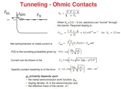
An ohmic contact is when there’s an unlimited transfer of majority carriers from one material to another.1,7 The contacts will not limit the current. Achieving such a contact is done by doping the semiconductor heavily enough to enable tunneling.
Ohmic substrate contacts lead to a very simple structure. Reference 1 demonstrates isolation capability and substrate noise coupling of ohmic substrate contacts within an HV CMOS technology (see figure).
Substrate coupling has been investigated for substrate contacts in a 0.35-µm HV CMOS process (Vmax ≤ 120 V, 20-Ω substrate, 0.5-Ω-cm pwell). It has been demonstrated that p+ guard rings can provide a quite good damping behavior. The isolation doesn’t strongly depend on the layout. For reliable measurements, additional metal pad shields are applied to suppress unwanted capacitive pad-to-substrate coupling.
Methods for Isolation of RF-SOI Devices
Shallow trench isolation (STI) will prevent current leakage between active semiconductor regions. This method makes it possible to scale device density. STI is created at the beginning of the device fabrication process, just before transistors are formed.
RF-SOI is the RF version of silicon-on-insulator (SOI) technology, which differs from fully depleted SOI (FD-SOI) for digital chips.5
Isolation can be created in two ways:
- Via an oxide growth between active shapes referred to as local oxidation of silicon (LOCOS).
- Etching the trenches, first by filling with dielectric and then removing excessive dielectric using a chemical-mechanical planarization. This is a chemical mechanical polishing (CMP)-based STI technique. CMP STI can be performed in three ways: direct, mask aligned (Process A), and self-aligned (Process B).
Isolating LV and HV Devices and Associated Circuitry
AT&T Bell Labs developed a 100-V process that enables IC designers to isolate low-voltage (LV) and HV circuitry.8 This technology is perfect for applications that need LV analog and digital to have signal processing and control circuitry, independently combined together with HV output drivers and buffers.
Read more articles in the TechXchange: Delving into EMI, EMC and Noise.
References
1. “Investigation of Substrate Noise Coupling and Isolation Characteristics for a 0.35µm HV CMOS Technology,” W.C. Pflanzl, E. Seebacher, 14th International Conference, Mixed Design (MIXDES) 2007, June 21-23, 2007.
2. “Investigation and Simulation of the Isolation Technology for 3300V RB-IGBT,” 2019 International Conference on Sensing, Diagnostics, Prognostics, and Control (SDPC), Lei Cui, Bijun Zhang, Pengfei Wu, Ruliang Zhang, Li Ma, Zhibin Zhao, Junmin Wu, Yufeng Qiu.
3. “A Novel Isolated Gate Driver Power Supply Method for Self-Powered SiC DC Solid-State Switch Using Thermoelectric Generation,” Lei Qi, Wantong Chai, Xiangyu Zhang, Liangtao Zhan, Wuyu Zhang, and Wei Li, IEEE Transactions on Industrial Electronics, Vol. 71, No. 1, January 2024.
4. “An Experimental Study on High-Frequency Substrate Noise Isolation in BiCMOS Technology,” Ping-Chun Yeh; Hwann-Kaeo Chiou, Member, IEEE; Chwan-Ying Lee; John Yeh; Denny Tang, Fellow, IEEE; and John Chern, IEEE Electron Device Letters, Vol. 29, No. 3, March 2008.
5. “STI Techniques for Isolation of RF-SOI Devices Siva P Adusumilli,” Steven M. Shank, John Ellis-Monaghan, Chu-hsiang Teng, Mark D Levy, Anthony K Stamper, IEEE 2017.
6. “Process dependence of 0.11 μm RF CMOS on high-resistivity substrate for System on Chip (SOC) Application,” T. Ohguro, K. Kojima, N. Momo, H. S. Momose and Y. Toyoshima, Center for Semiconductor Research and Development, Toshiba Corporation, Semiconductor Company, 2008 IEEE Radio Frequency Integrated Circuits Symposium.
7. “Metal/Semiconductor Ohmic Contacts,” EE311 notes/ Saraswat, Stanford University, 2005.
8. “Integrable high voltage CMOS: Devices, process application,” W. G. Meyer, G. W. Dick, K. H. Olson, AT&T-Bell Laboratories, IEDM 85–733.
9. Shallow Junctions & Contacts, slide 34.


