Handling High Power Density in Additive Manufacturing
What you’ll learn:
- Challenges when dealing with high-power-density designs.
- Utilizing cloud manufacturing platforms (CMPs).
- Power packaging using additive manufacturing.
Today’s designers are now more equipped to achieve high power density in power electronics applications. One excellent example of this is a method known as additive manufacturing (AM). A flyback AC-DC power converter using AM needs three-dimensional (3D) integration for passive and active components, particularly when working with industry-standard parts.
3D printing makes it possible for designers to produce the flexibility to construct diversified plastic carriers from varied materials, but without the need for expensive tooling. And, still, it enables complex structures for thermally, electrically, and mechanically improved setups.
Dealing with Higher Temperatures and Manufacturing of a 10-W Power Converter
We will endeavor to present a three-dimensional, integrated, 10-W AC-DC flyback converter example that employs AM and compare it to a conventional planar printed-circuit-board (PCB) technique. An additive-manufactured plastic structure will combine the qualities of a heatsink, isolator, and mechanical linkage. In addition, passive components can be optimized in volume through a rigorous selection process.2,8
The ceramic capacitors6,7 for such a power converter are important in this design as well: Their cuboid shape is perfectly suited for a high degree of 3D integration while parasitic losses are reduced when compared to electrolytic capacitors.
>>Download the PDF of this article, and check out the Library Series for similar articles and videos
To achieve efficient component placement along with a sufficient power-dissipation budget, the flyback converter housing is cube-shaped with structured surface. All active and passive components are completely enclosed in the plastic additive-manufactured structure, which improves the thermal connection. To avoid internal and surface hotspots, the filament positioning and selection of the heat sources are optimized via thermal 3D-FEM simulation.
Utilizing Cloud Manufacturing Platforms (CMPs)
Many existing approaches in modern research are able to optimize central platform concepts, open them for different domains, or even operate them as decentralized concepts. However, in any industrial environment, implementation of these concepts is limited.10
A series of studies exist that can analyze an available range of functions. This analysis covers the area of AM via the four most common technologies of fused deposition modeling (FDM), polymer powder bed fusion selective laser sintering (SLS), vat polymerization stereolithography (SLA), and metal power bed fusion selective laser melting (SLM). It provides an overview of the quality of the available CMPs in the field of AM.
In the search for the CMP that fits best, providers revealed that the features and parameters (functional properties) for the most important criteria were at 40%. This is due to the need to highlight the technical innovation behind the individual platforms.
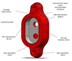
Let’s look at the component of a pump housing for the FDM manufacturing process (Fig. 1). In its original orientation, the pump-housing placement wasn’t optimally positioned on its hollow front side so as to force the printing of support structures or optimization processes.
ABS was chosen as the common material and nylon P6 as the uncommon. A solid with such a large circumference causes additional warping, which will typically require a heated printing chamber. The resolution of the print was done at a standardized height of 0.2 mm.
Power Packaging with AM
The industry is developing advanced AM processes and materials that are enabling low-cost production with improved SWaP-C power packages.5,8 The benefits are:
- Increased power density
- Lower inductance
- Improved reliability
- Cost-effectiveness for low-volume production
- Customized power substrates
- Thermal transient suppression
- Integrated substrate—heatsink
- Disruptive design space
- Complex internal features
- Functionally graded materials
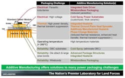
Overall, additive manufacturing provides solutions to power packaging challenges (Fig. 2).
AM Applications for Thermal Management in Power Electronics
Today’s thermal management has limitations when employing conventional methods for manufacturing. The implementation of AM will help to improve thermal management.5,8
Increased heat flux and reduced wide-bandgap (WBG) device packaging is pushing power electronics technology to achieve more effective thermal-management solutions with tighter weight and volume constraints.
Additive Manufacturing for Development of a Power Module
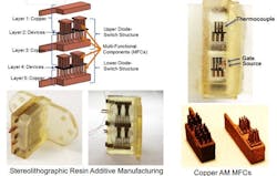
The U.S. Army has a need for electrical power in the battlefield. Packaging of such power devices will typically have higher power and smaller size, which leads to a significant rise in temperature. Improved packaging technology along with better cooling techniques will be needed in the future (Fig. 3).
A full three-phase inverter for an AM power module will reduce weight and size by 8X, in addition to a 5X to 10X reduction in the package thermal resistivity (Rth = 0.25 Kcm2/W).
Rth is defined as the ratio of the change in device temperature (ΔT) to the electrical power applied (P) and is expressed in °C/W or K/W
How AM Assists in Power-Component Manufacturing
A system-level approach for the design of power electronics devices should be performed so that designers will fully be able to face the challenges of higher power density and improved efficiency in their power-system designs.
More advanced packaging and system integration leads to improved compact designs; however, this effort will result in thermal management and component manufacturing complexities. Additive manufacturing will help mitigate some of these difficult challenges.
References
1. “Beyond the Surface: The Power of Density Determination in Additive Manufacturing” (automation.com).
2. “Additive Manufacturing of 10 W Power Converter with High Power Density,” Daniel Dell, Julian Weimer, Ingmar Kallfass, EPE'21 ECCE Europe.
3. “Process based modelling of power density for wire laser additive manufacturing using a coaxial head,” Clément Roch, Christophe Tournier, Sylvain Lavernhe, Additive Manufacturing, Elsevier, Volume 73, July 5, 2023, 103648.
4. “Additive Electronics: Next-Gen 3D Semiconductor Packaging,” David Ramahi, Additive Manufacturing, 2023 (We send our sympathy to the family of David Ramahi who passed away in March 2023).
5. “Current and Potential Applications of Additive Manufacturing for Power Electronics,” Luis Lopera, Romina Rodriguez (Member, IEEE) Mostafa Yakout, Mo Elbestawi, and Ali Emadi (Fellow, IEEE), IEEE Open Journal of Power Electronics, January 2021.
6. “Applying Ceramic Tech to Achieve High Power Density (Part 1),” Steve Taranovich, Electronic Design, July 23, 2023.
7. “Applying Ceramic Tech to Achieve High Power Density (Part 2),” Steve Taranovich, Electronic Design, July 20, 2023.
8. “Additive Manufacturing in Power Module Development,” Dr. Lauren Boteler, Dimeji Ibitayo, Morris Berman, Mike Fish, Claude Pullen, Marco Echeverria, University of Puerto Rico at Mayaguez (UPRM), 3D PEIM, June 2018.
9. The Fourth International Symposium on 3D Power Electronics Integration and Manufacturing (3D PEIM), February 1-3, 2023.
10. Study on Available Cloud Manufacturing Platforms for Additive Manufacturing Technologies, 4th IEEE Eurasia Conference on IoT, Communication and Engineering 2022, Matthias Milan Strljic, Islam Younes, Oliver Riedel.


