Mitigating and Measuring EMI Disturbances at IC Inputs
- Definitions of the electromagnetic emission (EME) with integrated circuits.
- Challenges of EMI in modern ICs.
- Some innovations in low-voltage ICs for Improved EMI immunity.
In these modern times, electronic systems are usually operating within an electromagnetic-interference (EMI) environment that contains many other electronic systems. These systems need to exist and fully operate undisturbed while meeting electromagnetic compatibility (EMC).
Overview of Electromagnetic Compatibility
EMC requirements are separated into two main parts:
- Electromagnetic immunity—a system must not be disturbed by any other systems.
- The electromagnetic interference in a system can’t disturb any other system.
Then, if immunity and emission requirements are individually met, the electronic product, such as an integrated circuit (IC), may be marketed from an EMC point of view.
Standard Measurement Techniques for ICs
Measurement methods for EMI and electromagnetic emission (EME) are fully described for ICs in the IEC62132-4 (immunity) and IEC61967-4 (emission) standards.1
Now let’s characterize the EME at one of the IC pins while injecting a radio-frequency (RF) disturbance signal into another IC pin. To do this, we can use a combination of two widely used IC measurement techniques:
The 150-Ω method (IEC 61967-4)
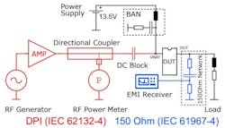
The 150-Ω technique is a generally adopted approach selected to measure conducted electromagnetic emissions. It uses an impedance-matching network that consists of a 6.8-nF decoupling capacitor in series with a 120-Ω resistor and one 51-Ω resistor in parallel to the input of the EMI receiver. This will lead to an approximate impedance of 150 Ω for the device under test (DUT), in addition to a good matching for the input impedance of the EMI receiver.
>>Download the PDF of the article, and check out the TechXchange for similar articles and videos
The deep packet inspection (DPI) method (IEC 62132-4)
The DPI method is an accepted approach chosen to simulate EMI caused by field coupling in antenna structures such as printed-circuit-board (PCB) traces or cables. This method involves the injection of a disturbance signal directly into an IC pin. The DPI is performed via an RF signal generator, which is generating the disturbance signal, and a power amplifier that will increase the power levels to meet the requirements of automotive test standards.
Both techniques offer highly reproducible and easy-to-use methods. Readers can see the complete setup as shown in Figure 1, with the DPI in red and the 150-Ω network in blue. By combining the two stages of the test procedure, it’s conceivable to measure the EME at its output along with injecting a disturbance signal into the battery pin.
Moreover, the use of coupling networks, which are based on standards, assures that the test procedure is comparatively easy to perform while displaying excellent reproducibility.
The DUT in Figure 1 is an automotive smart-power high-side switch. These types of components are typically used to control the vehicle headlights or switch the indicator lights. The device is operated in the switching mode via a switching frequency of 100 Hz along with a 50 % duty cycle. As a substitute for a car headlight, designers may choose to use a simple resistive load at the output. The disturbance is injected into the supply (VBAT) pin of the DUT.
Challenges of EMI in Modern ICs
A novel CMOS ultra-low-voltage (ULV) current bias solution offers a way to properly source ICs that are operating in subthreshold regions even in the presence of EMI.7
Power-supply reduction and scaling heightens susceptibility to EMI in ICs. The presence of disturbance can influence the behavior of analog building blocks—an issue that’s become increasingly critical. The nominal IC behavior must be guaranteed in every operating condition; EMI filters can’t be used since their presence may affect nominal circuit operation.
Among the fundamental IC building blocks, the susceptibility of current sources of ULV ICs creates quite a difficult task due to their reduced noise margin. However, a new current bias method presented below delivers higher EMI immunity with respect to existing current-mirror schemes.
Innovations in Low-Voltage ICs for Improved EMI Immunity
Technology trends in scaling and power-supply reduction have led to increased EMI susceptibility of ICs.5
Addressing this issue, a new CMOS ULV current bias solution for properly sourcing ICs that operate in subthreshold, even in the presence of EMI. The susceptibility of the current source of ULV ICs, including building blocks like the current splitter and current correlator, is a daunting task due to their reduced noise margin.
The robustness of the proposed EMI solution may be compared to conventional current mirrors. It’s evaluated via analytic methods and time-domain simulation, with reference to the AMS C35 0.35-µm CMOS technology process, to prove the solution’s higher EMI immunity to EMI.
Figure 2 represents the N- and P-type current mirrors, which include a low-pass filter (RFCF), to highlight the EMI-induced current. The DC offset is named Δn (Fig. 2a) and Δp (Fig. 2b).
The above-mentioned circuitry, operating in subthreshold, are selected as building blocks for a new current biasing circuit depicted in Figure 3. The circuit provides an output current IOUT (in the range of hundreds of nanoamperes and below) that’s suitable for an EMI-robust, ultra-low-power IC. This is the case even if the input current IIN is affected by EMI (iemi).
The presence of complementary N- and P-type current splitters in Figure 3 support the rapid scaling of the input current. They offer the significant benefit of an EMI-induced offset compensation based on an N-P offset compensation, which is performed through the current correlator.
The scaled currents coming from N- and P-type current splitters will flow to the respective current correlator that balances the opposite offset trend according to Equation 1:
IOUT = KCC ∙ I/2 (1)
If we assume that the aspect ratio of the current correlator equal to KCC = 2, then:
I = IIN/KCS (2)
Equation 2 acts as a current mirror-like function that’s exceedingly immune to EMI for low-power-consumption ICs operating within the nanoampere region.
RFI Susceptibility
To verify the EMI strength of the proposed circuit solution, time-domain simulations were performed with reference to the AMS C35 0.35-µm CMOS technology.
Analyses were required referring to a traditional current mirror in Figure 2a and the proposed solution in Figure 3. For both current bias methods, the output current IOUT = 200 nA is carried out by an input current IIN = 10 µA affected by a continuous-wave (CW) RF current iemi. The interference current iemi is overlapping the input current IIN and the DC offset on the output current IOUT is treated equivalently to immunity tests.
Summary: Saving Time and Cost with Low-EMI Solutions
Engineers creating low-EMI designs will be able to shorten development cycle time, lower the cost of the solution, as well as the design board area. Some tried-and-true techniques developed by Texas Instruments use the company’s EMI-optimized power-management devices. This helps certify that designs using TI components will pass industry standards with a minimum of rework.
References
1. “A Method to Measure the Electromagnetic Emission Induced by Electromagnetic Interference of Integrated Circuits,” Daniel Kircher, Nikolaus Czepl, Dominik Zupan, Bernd Deutschmann. Institute of Electronics (IFE), 2023 Joint Asia Pacific International Symposium on Electromagnetic Compatibility and International Conference on ElectroMagnetic Interference & Compatibility (APEMC/INCEMIC IEEE 2023).
2. “Time-Saving and Cost-Effective Innovations for EMI Reduction in Power Supplies,” Yogesh Ramadass, Ambreesh Tripathl, Paul Curtis. Texas Instruments, December 2023.
3. “One-Chip Active EMI Filter With Integrated Buck Converter and Self-Malfunction Detection for CE Noise Reduction,” Sangyeong Jeong and Jingook Kim, Senior Member, IEEE. IEEE Transactions on Power Power Electronics, Vol. 38, No. 11, November 2023.
4. “On-Chip Condition-Adaptive Δ f3 EMI Control for Switching Power ICs,” Lixiong Du, Student Member, IEEE, Dong Yan, Member, IEEE, and D. Brian Ma, Senior Member, IEEE. IEEE Journal of Solid-State Circuits, Vol. 58, No. 12, December 2023.
5. “Ultra-Low Voltage Current Biasing Highly Immune to EMI,” Orazio Aiello, Department of Electronics and Telecommunications, Politecnico di Torino, Torino, 10129, Italy, ICSyS2019 1570572817.
6. “Identification of EMI Induced Changes During the Design of ICs using a Post-Processing Framework,” Dominik Zupan, Bernd Deutschmann. Institute of Electronics (IFE), Graz University of Technology, SMACD 2019, EDA Competition, Lausanne, Switzerland.
7. “Analysis and Design of Analog Integrated Circuits Lecture 16, Subthreshold Operation and gm/Id Design,” Michael H. Perrott, April 1, 2012.
8. “Introduction to EMI: Standards, Causes and Mitigation Techniques,” Technical Article, Yogesh Ramadass. SSZT173, Texas Instruments, April 2021.


