How to Model, Measure, and Reduce EMI Noise
What you’ll learn:
- EMI standards needed to ensure compatibility.
- EMI reduction methods that can be applied to power modules.
This article offers ways to reduce and even avoid electromagnetic interference (EMI)—noise—in their designs. We’ll look at some electronic system design examples plagued or even damaged by EMI and some tried and true methods of reducing or even eliminating harsh EMI disturbances.
EMI Noise Modeling
Two common-mode (CM) noise sources make up the CM noise model of the three-level T-type inverter (3LT2I) used in adjustable-speed-drive (ASD) systems.5 The 3LT2I holds some significant advantages over a two-level voltage source inverter (2L-VSI), including:
- Silicon-carbide (SiC) MOSFETs allow for switching at higher voltage and current.
- SiC MOSFETs enable low switching losses and higher operating temperatures.
The SiC MOSFET’s fast switching speeds generate high-voltage slew rates, i.e., high dv/dt. This will create more EMI challenges, along with higher bearing currents in the motors, leading to deterioration in the insulation of the motor windings.
A couple of EMI standards, such as EN 50121 and IEC 61800, provide the limits of EMI emissions, which can ensure that the system will be electromagnetically compatible within its environment. The EMI noise modeling of the 2L-VSI has been widely conducted, as seen in literature.
>>Download the PDF of this article, and check out the TechXchange for similar articles and videos
Each phase of a 2L-VSI has just one voltage varying node. However, the three-level neutral point clamped (3L-NPC) maintains three voltage varying nodes while the 3LT2I has two voltage varying nodes. Unfortunately, the increase in voltage-varying nodes tends to complicate the EMI modeling of the three-level inverter topologies.
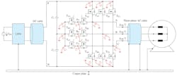
Many models of the three-level inverter (mainly with the 3L-NPC) focus on grid or photovoltaic applications. Unfortunately, no study has occurred for the EMI modeling of the 3LT2I for any ASD system (Fig. 1).
Using the EMI Reduction Method for Power Modules
High-power integrated power modules have a very compact design with a high dv/dt slew rate. These kinds of power modules are quite susceptible to EMI.7
Designers have proposed using a vertical module design, which displays improved EMI performance, over a wire-bonded module. Another proposed concept involves a novel EMI simulation method that utilizes ANSYS EM tools.
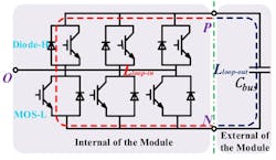
We can analyze the EMI mechanism of a complete SiC MOSFET integrated power module by examining the EMI coupling paths in both CM and differential-mode (DM) interference (Fig. 2).
The upper and lower devices within the phase leg module are made up of three bare-die MOSFETs in parallel along with three anti-paralleled diode bare dies. The largest current loop is made up of DIODE-H and MOS-L, which have the highest overvoltage and the maximum loop inductance. We find that the overvoltage of the power devices will increase the EMI in the high-frequency domain.
So, from Figure 2, the upper and lower devices within the phase leg module are made up of three paralleled MOSFET bare die. We can see that the largest current loop is made up of MOS-L and DIODE-H; this has the highest overvoltage with the maximum loop inductance. Unfortunately, the overvoltage of the power devices would increase the EMI within the high-frequency domain.
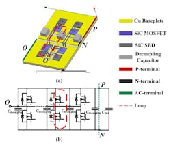
We now must decrease the large loop inductance that dominates the EMI in the high-frequency domain. What’s proposed is a packaging structure with an adjacent decoupling concept that has many split decoupling capacitors, which will be between the power devices (Fig. 3). The 3D model in Figure 3 identifies a smaller current loop path.
Simulating the Power Module
Finally, a simulation methodology that organizes co-simulation techniques, using ANSYS EM tools, predicts radiated and conducted EMI from the power electronic module. A synchronous buck converter is simulated via ANSYS Simplorer software. It’s able to import the electrical parameters of the full-SiC power module from the ANSYS Q3D software. A commercial, complete SiC MOSFET integrated power module, and a self-created one, are tested and compared, which verifies the EMI model method.
References
1. “Develop Common-Mode EMI Noise Models for AC-DC-AC Traction Systems,” Le Yang, Hui Zhao, and Shuo Wang, University of Florida; Yongjian Zhi, Bingquan Zhu, and Jianjun Min, CRRC Zhuzhou Institute Co., Ltd., IEEE 2017.
2. “EMI Measurement and Reduction for SiC MOSFET based Motor Drivers of Electric Vehicles,” Yunlei Zhang, Jiandong Guo, Haiming Liu, Xu Zhang, Yun Wang, Yan Fan, 2023 3rd International Conference on Electrical Engineering and Mechatronics Technology (ICEEMT).
3. “Driving of a GaN Enhancement Mode HEMT Transistor with Zener Diode Protection for High Efficiency and Low EMI,” O.C. Spro, S. Basu, I. Abuishmais, O.-M. Midtgård, and T. Undeland, EPE'17 ECCE Europe.
4. “Investigation and Reduction of a Low-Frequency EMI Noise of AC/DC Power Adapters with Diode Bridge as Input Rectifier,” Zhedong Ma, Yiming Li, and Shuo Wang, University of Florida; Honggang Sheng, Srikanth Lakshmikanthan, and Doug Osterhout, Google Inc. Hardware Team, 2020 IEEE 9th International Power Electronics and Motion Contral Conference (IPEMC2020-ECCE Asia).
5. “Common-Mode EMI Noise Modeling of Three-Level T-Type Inverter for Adjustable Speed Drive Systems,” Vefa Karakasli, Abdelmoumin Allioua, and Gerd Griepentrog, Technical University of Darmstadt Institute for Power Electronics and Control of Drives, EPE’22 ECCE Europe, and IEEE.
6. “Modulated Model Predictive Speed Control for PMSM Drives,” Cristian Garcia and Jose Rodriguez, Universidad Andres Bello Santiago, Chile; Shafiq Odhano and Pericle Zanchetta, University of Nottingham, Nottingham, UK; S. Alireza Davari, Shahid Rajaee, Teacher Training University, IEEE 2018.
7. “An Advanced Design of Power Module with EMI Reduction Method,” Xiliang Chen, Wenjie Chen, Yu Ren, Liang Qiao, Xu Yang, IEEE 2018.


