The Role of Snubber Circuits in Modern Switching Technologies
What you’ll learn:
- The critical role of snubber circuits in minimizing ringing and overshoot.
- How snubber circuitry is evolving to adapt to trends in power electronics, like the rising interest in wide-bandgap semiconductors.
Switching devices and their supporting circuitry continue to advance to meet the demands of an ever-evolving power-electronics landscape. With the rise of silicon-carbide (SiC) and gallium-nitride (GaN) wide-bandgap semiconductors alongside silicon IGBTs and silicon MOSFETs, there are new (read: higher) expectations of power converters and inverters.
Rapid switching capabilities, high-voltage thresholds, and high efficiency are significant benefits, but they require a nuanced approach to managing the accompanying high-frequency parasitics. This article explores how the evolution of switching technologies is influencing snubber circuitry.
Snubber Circuits and Their Functional Role
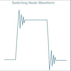
Even a perfectly designed printed circuit board (PCB) has parasitic capacitances and inductances. Their effects can impact PCB operations if not considered in the layout. For example, in a converter with higher switching frequencies (Fig. 1), overshoot and ringing are likely if one doesn’t account for component selection and implementation.
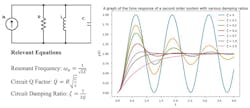
Overshoot describes the scenario when the output of a filter has a higher maximum value than the input in a step response. Ringing artifacts result from sudden changes in voltage and/or current when switches turn on or off. For example, consider a DC-DC converter circuit, where the parasitic inductances and capacitance can be found in the board traces, field-effect transistor (FET) packaging, and individual passive components (Fig. 2).
If the DC-DC converter is designed with long stretches of wiring, it increases inductance. This condition, combined with larger current flow, generates high voltage. If the rise and fall time of the switching MOSFET are short, current and voltage are both large.
The advantages of this condition include reduced transition losses and increased efficiency, but it also makes the circuit more susceptible to high-frequency ringing when a switch is flipped on or off. In short, parasitic capacitances and inductances cause RLC circuits to respond differently to a step response under different damping conditions (Fig. 3).
One way to reduce overshoot and ringing is to implement energy-absorbing snubber circuits. Snubber circuits are aptly named as they’re designed to dampen or “snub” these effects when a mechanical or semiconductor switch opens by offering an alternate path for current.
The most popular design for these circuits includes a capacitor with a series of resistors connected across a switch. For example, adding an RC snubber network across a transistor (e.g., low-side MOSFET) can nearly eliminate parasitic ringing.
That said, there are several ways to reduce voltage overshoot and ringing. For example, with DC-link devices that can be placed closer to switches, the snubber function can be integrated with the DC-link function to decrease high-frequency ringing without increasing switching loss.
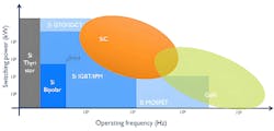
Just as there are several ways to implement snubbing effects, there are different kinds of switches with wide-ranging operating and switching frequencies—and the breadth of variety extends to snubber circuits. Different semiconductors are warranted depending on the power demands of the application (Fig. 4).
In some industries, like electric vehicles (EVs), SiC and GaN wide-bandgap semiconductors are attractive replacements for IGBTs and MOSFETs because they offer benefits like higher efficiency, better thermal performance, and faster switching speeds.
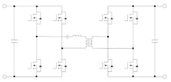
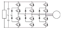
For instance, we’re seeing GaN wide-bandgap semiconductors in the multi-level converters found in EV onboard chargers (Fig. 5). Multi-level converters leverage switched-capacitor blocks connected in series. Different combinations of blocks can be used to form a desired waveform, making it possible to generate higher-voltage waveforms using lower-voltage components. With more switches, there’s a greater need for snubber circuits to eliminate parasitic effects.
Designing and Implementing Snubber Circuits
Running a switching device at the very edge of its performance calls for a meticulously optimized snubber circuit, which requires evaluating all circuit parameters, including specific component values and parasitic terms. That said, a couple of analysis methods can be applied to estimate snubber circuits by measuring or modeling what’s in and around the circuit.
Optimal design relies on detailed analysis. It requires knowledge of the AC characteristics of the circuit and balancing the snubber capacitance between the energy stored in the parasitic inductance and the switching speed of the semiconductor, which relates to the switching frequency.
CDE Cornell Dubilier points out that when power dissipation isn’t crucial to your design, there’s a quicker option. You can estimate snubber capacitance based on power rating, switching frequency, and voltage. This approach is founded on the idea that snubber capacitance requirements decrease as frequency increases.
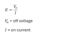
Implement a 2-W carbon composition resistor with a value that accommodates the pre-switch current value without voltage overshoot once the switch opens and current flows into the snubber circuit. Calculate the maximum resistance by dividing the voltage across the switch (VO) by the current value just before the switch opens (I).
According to Ohm’s Law:
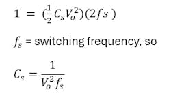
The resistor’s power dissipation is a function of the energy stored in the snubber capacitor and the frequency of voltage transitions rather than the resistance value itself. To snub the switch, you can choose the capacitance that causes the 2-W resistor to dissipate half of its power rating (i.e., 1 W):
All approaches to snubber-circuit implementation rely on measurement. Therefore, snubber-capacitor selection hinges on a deep understanding of the switching device and its surroundings. As switching devices evolve toward ultra-wide-bandgap filters and other unique materials, snubber circuits need to evolve, too. There’s no one-size-fits-all solution. For high-performance applications, there must be a clear line of communication between the circuit designer and the capacitor manufacturer.

