Use an LDO and PLD for Power-Supply Enable and Disable Functions
What you'll learn:
- The enable controller setup and its features.
- What is the TPLD801-Q1 PLD?
- Test results for the combined PLD/LDO solution.
- Why a PLD/LDO combo is better than an MCU for power-supply enable and disable.
Many systems require enabling and disabling through control lines or when applying the input power. While a small microcontroller (MCU) can implement the enable/disable function, you still need to write, maintain, and flash code for it. Many designs using a system-on-chip (SoC) have an MCU within that chip; adding another is redundant. Moreover, the MCU in the SoC isn’t low power enough to both remain always on and provide the enable controller function.
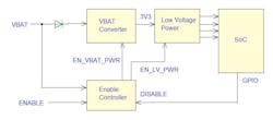
This article discusses a low-cost, low-power enable controller hardware solution that consumes only microamperes of current using a low-dropout linear regulator (LDO) plus a programmable logic device (PLD). The PLD comes preprogrammed with the logic you need to implement the decision-making function of the enable controller. Figure 1 shows the proposed solution; its power supplies are typical for an automotive system powering an SoC.
Enable Controller Solution
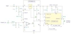
This solution employs the TPS7B85-Q1 off-battery LDO1 and the TPLD801-Q1 PLD2 (Fig. 2). Features in the TPS7B85-Q1 are specifically useful in this application:
- The basic LDO function provides a fixed 3.3- or 5-V output voltage (VOUT) from a battery voltage (VBAT) of up to 40 V. This VOUT provides power to the TPLD801-Q1.
- A power-good (PG) output with pin-programmable delay. When applying VBAT, the LDO powers up. When the LDO VOUT reaches regulation, PG goes high after a delay programmed by a capacitor on the DELAY pin. The TPLD801-Q1 uses the rising PG signal to detect and latch an initial application of VBAT (FIRST_EN) to enable the system.
- An uncommitted SENSE comparator provides a logic high or low sense output (the SO pin) if its sense input pin (the SI pin) is above or below the 1.21-V internal voltage reference (VREF), respectively. The SI pin has a maximum voltage of 40 V irrespective of whether the LDO VIN is powered or not. For blocking negative voltages, you can use diode D2. The comparator tests whether the ENABLE_IN signal’s amplitude is above a certain voltage threshold. If it is, then the signal is allowed to pass to the TPLD801-Q1’s enable input. This voltage threshold is adjustable through R4 and R5.
- A precision enable (EN) pin. The precision enable feature (as opposed to logic level enable) isn’t documented in the TPS7B85-Q1 datasheet, but the EN pin goes to a comparator with a 1.32-V VREF threshold (rising) and hysteresis of 100 mV. It allows for the use of a resistor divider (R2, R3) from VBAT to EN to ground to set a precise VBAT startup voltage. Using the precision enable ensures that the LDO’s output doesn’t ramp with rising VBAT (which has an unknown ramp rate), but waits until VBAT is above the set startup voltage before turning on the LDO. In this case, VOUT rises in approximately 240 μs, regardless of the VBAT ramp rate. With the resistor values shown, the VBAT startup voltage of the LDO is approximately 6.5 V, but it’s adjustable through R2 and R3. The ramp rate of VOUT is important because the TPLD801-Q1 has a maximum (slowest) allowable VCC ramp rate of 0.25 V/ms.
Bleed resistor R1 discharges the output capacitor of the LDO (C1) during power down. The TPS7B85-Q1 has 30-kΩ internal pullup resistors on its PG and SO pins. The length of the PG delay is a matter of choice. The CDELAY = 4.7 nF gives a delay of approximately 4 ms (Fig. 2, again).
>>Download the PDF of this article, and check out the TechXchange for similar articles and videos
Some Design Notes on the TPLD801-Q1
The TPLD801-Q1 is an automotive-qualified PLD, integrating logic blocks such as flip-flops, counters, delays, logic gates, and a 25-kHz or 2-MHz oscillator, as well as dividers and a pipeline delay. TI’s InterConnect Studio design tool can graphically design and simulate the logic design.
You can also use the TPLD801 evaluation module and TPLD programmer kit to permanently program the logic design into one-time programmable memory, or temporarily program the design into volatile registers.
At the heart of the TPLD801-Q1 logic design is a D-type flip-flop configured as a latch (ENABLE LATCH), so that the rising clock edge latches a logic-high output. Only the reset input can reset the latch. The latch output goes into two separate delay lines, each set to approximately 15 ms. When the latch output goes high, the EN_VBAT_PWR signal immediately goes high and enables the front-end power supply.
To allow time for the front end to power up first, the EN_LV_PWR signal goes high approximately 15 ms later and enables the power supplies powering the SoC and the rest of the system.
It’s possible to clock the ENABLE LATCH with a rising edge in two ways:
- At the first enable event, which generates a rising edge on the PG output of the LDO.
- With an ENABLE signal that’s been passed to the PLD from the TPS7B85-Q1’s SO output, and what the PLD has measured is longer than a pre-programmed duration. Alternatively, you could use an inverted ENABLE/ signal if you need a different application; but if unused, it’s tied high.
In the second instance, and for the purpose of rejecting spurious noise signals, the PLD measures if the incoming ENABLE signal is long enough by passing it through a delay line that’s clocked with the PLD’s internal 25-kHz, divided-by-four oscillator. The 25-kHz oscillator is very low power, consuming 8.2 μA.
The delay line count of 94 gives an approximate 15-ms total delay, although you can set this time to a different duration as required by the application. If the incoming ENABLE signal is still present during and after this delay, the output of the delay line goes high, which presents a rising edge to the ENABLE LATCH’s clock and latches a logic high. If the incoming ENABLE signal wasn’t present for the entire time, then the delay counter resets and the rising edge to the latch doesn’t occur.
When the electronic control unit needs to power down, the SoC’s MCU issues a rising edge through a general-purpose input/output. This DISABLE signal connects to the open-drain transistor shown in Figure 1 and pulls down the DISABLE/ pin of the PLD to reset the ENABLE LATCH. After the ENABLE LATCH resets, the EN_LV_PWR output goes low immediately; approximately 15 ms later, the EN_VBAT_PWR output goes low.
This 15-ms delay enables the low-voltage power rails to sequence down in the correct order required by the SoC before the front-end power supply becomes disabled. The delay times between EN_VBAT_PWR and EN_LV_PWR rising or falling are configurable by changing the count of the delay lines.
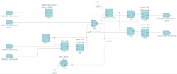
Selecting the PLD inputs to be Schmitt-trigger inputs provides leeway in how fast the logic signals driving into them need to transition. The two enable output signals are configured as push-pull. (If using open drain instead, then this configuration gives a glitch on power-up, as the open drain outputs are pulled momentarily high by the pullup resistors before the one-time programmable memory, OTP, of the TPLD801-Q1 has loaded and configured the outputs to be open drain. Even with push-pull, the outputs are high impedance before the OTP memory loads; thus, you may need external pull-down resistors.) Figure 3 shows the overall PLD design.
Bench Test Results for the PLD/LDO Combo
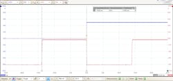
Figure 4 shows an 18-V ENABLE_IN signal applied to the enable controller, which certainly has an amplitude that makes it possible for the TPS7B85-Q1 comparator to pass it to the PLD. The signal also has a sufficient duration for detection being validated by the PLD. The ENABLE LATCH latches high in response to this ENABLE_IN signal and stays high even if the ENABLE_IN is toggled.
It’s possible to successfully repeat this test for a low-amplitude, 3.4-V signal at the other extreme. Or you can repeat the tests for short duration, low-amplitude ENABLE_IN signals, or both, which are insufficient in duration or amplitude to trigger the ENABLE LATCH to be high.
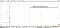
Figure 5 illustrates the behavior of the circuit when first applying the input power to the LDO. The PG pin goes high when the LDO regulates, and after a delay (set by CDELAY), the first power-on event is detected by the PLD and the ENABLE LATCH latches high. (This test used the default 1-μF CDELAY capacitor of the evaluation board, which gives a much longer delay.)
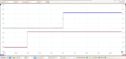
The actual outputs of the PLD are shown in Figure 6, including an approximate 15-ms delay during the power-up sequence.
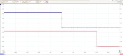
Figure 7 shows the PLD outputs during a DISABLE event, depicting the 15-ms delay.
Why the PLD/LDO Combo is Better than a Microcontroller
This low-cost and low-power, hardware-based solution for handling power-supply enable and disable functions removes the need for an external MCU and can be further customized. You also have the option of ordering a custom PLD with the logic design pre-programmed on it.
A pre-programmed PLD avoids the time and cost of writing and maintaining firmware for an MCU. Moreover, it avoids having to program an MCU in your production environment. These time-saving features of having the pre-programmed PLD and the fact that the TPLD801-Q1 and TPS7B85-Q1 hardware solution is low cost saves overall system expense.
The TPLD801-Q1 is available in a small package measuring 1.6 × 2.1 mm and the TPS7B85-Q1 comes in a 3- × 3-mm package, which saves space in the overall printed circuit board layout. This is helpful to printed-circuit-board designers who often face the task of having to fit more functionality into the same board area.
Acknowledgement: The author wishes to thank Thijs Tooth for his assistance in the bench testing of this circuit idea.
References
1. “TPS7B85-Q1 150-mA, 40-V, Low-Dropout Regulator with Power-Good and Integrated Voltage Monitoring.” Texas Instruments datasheet, literature No. SBVS360A, February 2020, revised November 2020.
2. “TPLD801-Q1 Automotive Programmable Logic Device with 6-GPIO.” Texas Instruments datasheet, literature No. SCPS301, September 2024.

