Printable Substrate Pushes Sensor Options Beyond Just Printing Electronics
Printable electronics with flexible circuitry deposited on a plastic substrate—the subject of research for decades—has seen modest success. However, commercial use remains limited. Now a team led by Subramanian Sundaram, a graduate student at MIT’s Computer Science and Artificial Intelligence Laboratory (CSAIL), is trying to go beyond just printing the active circuitry, using flexible, printable electronics that combine both sensors and processing circuitry. The printed substrate could consist of different substances interlocked in intricate but regular patterns, thus broadening the range of materials that can be used for printable electronics.
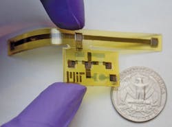
As proof of concept, they built a combined substrate/circuit device that responds to mechanical stresses by changing the color of a spot on its surface, as reported in Advanced Materials Technologies ("3D-Printed Autonomous Sensory Composites"). The device is shaped roughly like a T (see figure) with a wide base and an elongated crossbar.
The crossbar is made from an elastic plastic with a strip of silver running its length, and electrodes were connected to the crossbar’s ends. The base of the T is made of a more-rigid plastic with two printed transistors and what the researchers call a “pixel.” The pixel is a circle of semiconducting polymer whose color changes when the crossbars stretch, thus modifying the electrical resistance of the silver strip.
A technique being pioneered at MIT prints not only the active electronics, but also the supporting substrate, thus potentially enabling a fully integrated sensor/circuitry pairing and use of optimized materials for each function. (Source: MIT)
The transistors and the pixel are made from the same material, and the transistors change color slightly when the crossbars stretch. However, the pixel shows the stretching more dramatically because the transistors amplify the minute electrical signal from the crossbar. Demonstrating working transistors was critical, Sundaram noted, because multisensor arrays will require some onboard signal pre-processing rather than simply streaming the raw acquired data to an associated processor.
The printed transistor consists of semiconductor channel above which is a “gate”—a metal wire that, when charged, generates an electric field that switches the semiconductor between its conductive and nonconductive states. These transistors separate the gate and the semiconductor with a layer of water containing a potassium salt. Charging the gate drives potassium ions into the semiconductor, which then changes its conductivity.
As with most new devices, the path from concept to actual fabrication is daunting. The researchers used a custom 3D printer previously developed by the group. The printer includes two different “print heads,” one for emitting hot materials and one for cool, plus an array of ultraviolet LEDs to “cure” fluids deposited by the print heads, thus producing the substrate. They added a copper-and-ceramic heater, which was necessary to deposit the semiconducting plastic.
This plastic is suspended in a fluid that’s sprayed onto the device surface. Then the heater evaporates the fluid, leaving behind a layer of plastic only 200 nm thick. The layer of saltwater lowers the device’s operating voltage to 1.5 V, but also makes it less stable.
“I think we can probably get it to work stably for two months, maybe,” says Sundaram, adding that “one option is to replace that liquid with something between a solid and a liquid, like a hydrogel.”


