When I was doing the National Semiconductor Analog Seminar with Bob Pease back in 2003 (Fig. 1), I gave a talk about rail-to-rail amplifiers. I stated that there were two ways to make a rail-to-rail amplifier. One is to use dual differential pairs in the input. The other way is to use a charge pump inside the IC so that the input stage operates at a higher voltage than the power supply to the amp. Pease heard this and corrected me. “There is a third way to make a rail-to-rail amplifier. Check out the LMC6482.”
1. The author and Bob Pease mug for the camera during the 2003 Analog Seminar held in America and Europe.
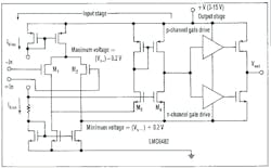
It turns out the LMC6482 and its quad version LMC6484 are magical parts still widely used. Its front-end stage uses MOSFETs (metal oxide field-effect transistors) hooked up in a very clever way. As the input pins swing from the positive rail to the negative rail, the FETs change type. They transmogrify from being depletion devices to being enhancement devices.
2. Don Archer, designer of the LMC6482, later a technologist for the Silicon Valley Analog group at Texas Instruments.
The LMC6482 was designed by Don Archer (Fig. 2), who recently left Texas Instruments. When the LMC6482 came out, Electronic Design did an article about it, currently unavailable online, on April 16, 1992 (Fig. 3). Back in 2003, I saw Archer in the cafeteria and asked about the part. A supremely modest fellow, he said it was no great accomplishment. “I just threaded the needle” when it came to biasing the depletion mode P-channel input-stage transistors so they would properly change from enhancement to depletion type as in the input voltage changed. Collaboration with the fab led to changes made on the process, which allowed for an enhanced body effect of the p-channel differential pair.
3. This figure from the 1992 Electronic Design article states: By using depletion-mode p-channel MOSFETs for the differential input transistor pair M1 and M2 in the LMC6482 CMOS op amp, the op amp can handle input common-mode voltages that exceed both supply rails.
The Inside Scoop
I had a chance to sit down with Archer in September of 2017, so I asked about the part. Still modest, he said the biasing scheme was not purely his effort. He based it on a suggestion from Dennis Monticelli, who later became CTO of National Semiconductor, now retired from Texas Instruments.
I emailed Monticelli for this article and he recalls, “The predecessor part was the LMC660, where rail-to-rail output was the prime feature along with input precision and gain that rivaled Bipolar or BiFet. I wanted to implement rail-to-rail on the input also, but the body effect was not great enough in our first-generation Si-gate process to pull it off. When Don took on the next-gen project, he convinced our Salt Lake fab to make a specific process change that provided the body effect he needed to thread that needle on the parallel input architecture.”
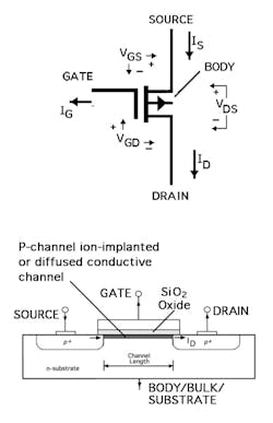
The trick Archer used to get rail-to rail inputs was to tie the body connection of the input FETs to the positive power-supply rail (Fig. 4). As the input pins swing down to the negative or ground rail, the bias across the body will change the FETs so that they become enhancement-type devices. This happens about 3 V below the positive rail.
4. Depletion-mode devices are normally on. You apply voltage to the gate to pinch off the channel. The LMC6482 ties the body connection to the positive rail, so the transistors change from depletion to enhancement as the input pins sweep the common-mode input range. (Courtesy of Linear Systems)
Who is Don Archer?
Archer was one of those wunderkinds that played with radios as a kid, as well as having a paper route delivering newspapers. He repaired typewriters and copy machines after graduating high school. A later job had him climbing smokestacks to repair and calibrate gas spectral absorption pollution monitors made by Thermo Electron Corporation. That gave him the impetus to go to California State University, Sacramento, where he earned a BSEE with a minor in physics. This would serve him well as an IC designer. In 1986, he was hired by National Semiconductor (now Texas Instruments), working in the hybrid group. While there, he obtained a Master’s degree from San Jose State University.
Archer told me, “You don’t survive without being flexible.” That and curiosity are hallmarks of an analog engineer. He also told me a good policy is to seek out knowledgeable people and to understand the boundaries and capabilities of devices so that you can get exemplary performance without “falling off the cliff.”
He noted that designing with circuit blocks invented by others is fine, but you must understand the blocks fully, or they can be dangerous. He said an analog IC designer must deal with thermal considerations, package stress problems, and noise issues. Archer reflects that you not only have to have reliable circuits, but the circuits have to maintain reliability under bias conditions as they operate.
Analog IC design appealed to Archer since the design is more focused on the physics of the transistor than is the case with digital circuits and “one designer gets to do everything.” He pointed out that for very low input bias current, electrostatic-discharge (ESD) protection is a big part of amplifier design. There’s also the problem that any design must have good yields in production, or it won’t be economical to produce.
Archer reminded me that working for a large company like National Semi or Texas Instruments creates a great responsibility to get things right. Back when he designed the LMC6482/84, the mainframe Spice level 2 model simulations did not give an adequate picture of the operation, so he did a piece-wise linear model of the transistors to make sure the simulation results reflected real-world part behavior. Sure, an analog IC designer is an electrical engineer, but also part physicist, to understand the silicon, and part computer scientist, to understand the design and simulation tools. It’s a tough job, but a rewarding one.
Like many clever IC designs, the LMC6482 design is based on a thorough understanding of the analog IC process used to make the die. An example of process and design working together was when the process development group at National Semi figured out how to put JFETs (junction field-effect transistors) into the analog process. This gave rise to parts like the LF411, one of Pease’s favorite parts.
Another example was when the audio group at National Semi (now Texas Instruments) figured out how to use a subset of devices to make the LME49720 audio amplifier that they characterized at 44 V to give a 36-V absolute maximum part rating. That’s better than the typical 30-V power-supply range of many high-voltage amps. This is important to audio folks, since a wide power-rail voltage tends to minimize distortion and improve specs, as well as provide a wide dynamic range for audio signals. Not all of the devices in the process would stand this voltage, but the IC designers worked with the process development group to figure out what transistors and structures could take this higher voltage, and then only used those devices in the part.
Other Methods Go Off the (Rail-to-)Rails
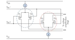
To understand the coolness of the LMC6482 and Archer’s achievement, consider the drawback of the other two methods of making a rail-to-rail operational amplifier. You can use a dual-input stage with both P- and N-type differential input pairs (Fig. 5). This works well if you have a circuit that operates with its inputs near either power-supply rail.
5. One way to make a rail-to-rail input amplifier is to have P-type and N-type differential pairs and gradually switch between the two as the input pins sweep the common-mode range. (Courtesy of Texas Instruments)
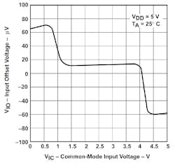
However, problems can occur when the input pins sweep across the transition zone. Since there are really two different differential pairs, the part will have two different offset voltages, depending on the location of the input pin voltage (Fig. 6). Worse yet, the particular offsets will be different for any given part, which may make it hard to achieve the accuracy you want. If the input stage is bipolar, the input bias current will also change from positive to negative as the inputs sweep across the common-mode range.
6. A problem with dual-input stage amplifiers is that the input offset voltage will change, depending on where the input pins are in the common-mode range. (Courtesy of Texas Instruments)
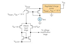
The other method, putting a charge pump inside the part, eliminates the problem of having two different offset voltages (Fig 7). Yet the charge pump has problems of its own. The charge pump needs on-die capacitors. This takes a lot of die area and will increase the cost of the part. The size of the capacitors will be related to the tail current of the input differential pair. So now the designer might want to use a low tail current to minimize the size and cost of the charge pump circuit.
7. Another way to make a rail-to-rail amp is to use just one input pair, but feed it with an internal charge pump so that the input pins work at both rails. (Courtesy of Texas Instruments)
The problem there is that the equivalent input voltage noise is inversely proportional to that tail current. The more you starve the tail current, the worse the noise performance of the part. In addition to the input noise is the noise of the charge pump itself. The switching frequency of the charge pump will invariably leak into the output of the amplifier. Usually this noise is at a greater frequency than the bandwidth of the amplifier, and you can filter it out. The filter circuit adds cost, complexity, and other issues, like stability and phase problems.
Another lecture for those analog seminars in 2003 was given by Martin Giles (Fig. 8). Like all of the presenters, Giles exhibited great intellectual honesty. While rail-to-rail parts were new and profitable, Giles would advise seminar attendees that they might not need one. If your circuit operates near the positive rail, you can look for amps with NPN or N-channel input pairs. If you want a circuit that operates near the negative rail (which might be ground), you can pick an old cheap amp that has a PNP or P-channel input.
8. Martin Giles was at the Analog Seminar in 2003. He reminded engineers they might not need a rail-to-rail part for many applications.
Rail-to-rail parts come in handy if your circuit must operate at both extremes. They can also make sense if you have two circuits that operate at each power rail, and you only want to buy and stock one part number. Just remember that each type of rail-to-rail part has its own quirks. You have to understand a little of what is inside the part to know if those quirks will bite you in prototyping or production. Bob Pease loved amplifiers, in part because they were so complex and, well, analog, despite only having a few pins.
